MB893 Socket LGA775 Pentium® 4 Intel® i915GV Chipset Server Motherboard USER’S MANUAL Version 1.
Acknowledgments Award is a registered trademark of Award Software International, Inc. PS/2 is a trademark of International Business Machines Corporation. Intel and Pentium 4 are registered trademarks of Intel Corporation. Microsoft Windows is a registered trademark of Microsoft Corporation. Winbond is a registered trademark of Winbond Electronics Corporation. All other product names or trademarks are properties of their respective owners.
Table of Contents Introduction .......................................................1 Checklist.............................................................................. 1 Product Description............................................................. 2 Specifications ...................................................................... 3 Board Dimensions ............................................................... 4 Installations .......................................................
The MB893 Server Motherboard iv MB893 User’s Manual
INTRODUCTION Introduction Checklist Your MB893 Pentium® 4 motherboard package should include the items listed below: • The MB893 motherboard • This User’s Manual • 1 IDE cable (40 pin 2.54mm) (optional) • 1 IDE cable (44 pin 2.
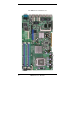
INSTALLATIONS Product Description The MB893 LGA 775 Pentium® 4 motherboard incorporates the Intel® i915GV chipset that can utilize a single LGA775 processor of up to 3.8GHz or higher and supports FSB frequency of 533/800MHz (133MHz, and 200MHz HCLK respectively). The i915GV chipset is designed for use with the Pentium® 4 processor with 1M Level 2 (CPU integrated) cache. The integrated MCH component provides the CPU interface, DDR interface and Hub Interface.
INTRODUCTION Specifications Product Name CPU Support CPU Voltage System Speed CPU Operating Frequency Green /APM CPU Socket Chipset MB893 Intel® Pentium® 4 0.8375V~1.6V (VRD 10.1) Up to 3.
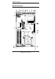
INSTALLATIONS Board Dimensions 4 MB893 User’s Manual
INSTALLATIONS Installations This section provides information on how to use the jumpers and connectors on the MB893 in order to set up a workable system. The topics covered are: Installing the CPU ................................................................................. 6 ATX Power Installation......................................................................... 7 Installing the Memory ........................................................................... 7 Setting the Jumpers.............
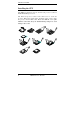
INSTALLATIONS Installing the CPU The MB893 motherboard supports an LGA 775 processor socket for Intel® Pentium® 4 processors. The LGA 775 processor socket comes with a lever to secure the processor. Refer to the pictures below, from left to right, on how to place the processor into the CPU socket. Please note that the cover of the LGA775 socket must always be installed during transport to avoid damage to the socket.
INSTALLATIONS ATX Power Installation The system power is provided to the motherboard with the ATX1 and ATX_12V1 power connectors. ATX1 is a 24-pin power connector and ATX_12V1 is an 8-pin 12V power connector. Note: The power supply 5VSB voltage must be at least 2A. Installing the Memory The MB893 motherboard supports four DDR memory sockets for a maximum total memory of 4GB in DDR memory type. It supports DDR333 when installed with CPUs that have clock speeds of 533MHz.
INSTALLATIONS Setting the Jumpers Jumpers are used on MB893 to select various settings and features according to your needs and applications. Contact your supplier if you have doubts about the best configuration for your needs. The following lists the connectors on MB893 and their respective functions. Jumper Locations on MB893.......................................................... 9 JP2: Compact Flash Master/Slave Select...................................... 10 JP3: Clear CMOS Contents ................
INSTALLATIONS Jumper Locations on MB893 Jumper Locations on MB893 ...........................................................Page c JP2: Compact Flash Master/Slave Select ........................................ 10 d JP3: Clear CMOS Contents............................................................. 10 e JP4: CN7 & CN10 LAN By-pass Function Setting ........................ 10 f JP5: COM2 (J6) Tx/Rx Signal Setting (Reserved) ......................... 10 g JP6: Case Open Connector (Reserved) .............
INSTALLATIONS JP2: Compact Flash Master/Slave Select JP2 Setting Compact Flash Open Slave Closed Master JP3: Clear CMOS Contents JP3 Setting Function Pin 1-2 Short/Closed Normal Pin 2-3 Short/Closed Clear CMOS JP4: CN7 & CN10 LAN By-pass Function Setting [ JP4 Setting Pin 1-2&3-4 OPEN Pin 1-2&3-4 Short/Closed (Default) Function System will bypass LANs upon the timeout of watchdog timer System will reboot upon the timeout of watchdog timer.
INSTALLATIONS JP6: Case Open Connector (Reserved) JP7: IDE1, IDE2 UDMA Cable Detect Setting JP7 Setting Function Pin 1-2 Short/Closed (Default) UDMA by cable detect Pin 2-3 Short/Closed UDMA33 Only MB893 User’s Manual 11
INSTALLATIONS [ Connectors on MB893 The connectors on MB893 allows you to connect external devices such as keyboard, floppy disk drives, hard disk drives, printers, etc. The following table lists the connectors on MB893 and their respective functions. Connector Locations on MB893.......................................................... 13 ATX1: ATX Power Supply Connector................................................ 14 ATX_12V1: ATX 12V Power Connector ...........................................
INSTALLATIONS Connector Locations on MB893 Connector Locations on MB893 ...............................................Page c ATX1: ATX Power Supply Connector ............................................... 14 d ATX_12V1: ATX 12V Power Connector ........................................... 14 e DIMM1,3: Channel A1,B1 DDR Socket............................................. 14 f DIMM2,4: Channel A2,B2 DDR Socket............................................. 14 g CPU_FAN1/2/3: CPU Fan Power Connectors ........
INSTALLATIONS ATX1: ATX Power Supply Connector Signal Name Pin # Pin # 3.3V 13 1 -12V 14 2 Ground 15 3 PS-ON 16 4 Ground 17 5 Ground 18 6 Ground 19 7 -5V 20 8 +5V 21 9 +5V 22 10 +5V 23 11 Ground 24 12 ATX1 is a 24-pin ATX power supply connector. Signal Name 3.3V 3.3V Ground +5V Ground +5V Ground Power good 5VSB +12V +12V +3.
INSTALLATIONS SYS_FAN1: System Fan Power Connector Pin # Signal Name 1 Ground 2 +12V 3 Rotation detection CN1: Front Side Bridge Board to ID370 Signal Name Pin # Pin # PWR-SW Reset-SW Speak VCC Ground HDD LED By-pass LED Ground Ground GPO0 GPO1 GPO2 GPO3 GPO4 GPO5 GPO6 GPO7 VCC GPIO32 GPIO33 GPIO34 VCC3 1 3 5 7 9 11 13 15 17 19 21 23 25 27 29 31 33 35 37 39 41 43 2 4 6 8 10 12 14 16 18 20 22 24 26 28 30 32 34 36 38 40 42 44 Signal Name 5VSB Ground VCC VCC PULL-UP PULL-UP PULL-UP Ground Ground GPI0 GPI1
INSTALLATIONS CN4: Mini PCI Socket Pin # Signal Pin # Signal Pin # Signal Pin # Signal 1 3 5 7 9 11 13 15 17 19 21 23 25 27 29 31 33 35 37 39 41 43 45 47 49 51 53 55 57 59 61 NC NC NC NC NC NC NC GND INTB# +3.3V NC GND CLK GND REQ# +3.3V AD[31] AD[29] GND AD[27] AD[25] 2 4 6 8 10 12 14 16 18 20 22 24 26 28 30 32 34 36 38 40 42 44 46 48 50 52 54 56 58 60 62 NC NC NC NC NC NC NC 63 65 67 69 71 73 75 77 79 81 83 85 87 89 91 93 95 97 99 101 103 105 107 109 111 113 115 117 119 121 123 +3.
INSTALLATIONS CN12: COM1 Connector CN12 (COM1) is a DB-9 connector Signal Name DCD, Data carrier detect RXD, Receive data TXD, Transmit data DTR, Data terminal ready GND, ground Pin # 1 2 3 4 5 Pin # 6 7 8 9 10 Signal Name DSR, Data set ready RTS, Request to send CTS, Clear to send RI, Ring indicator Not Used CN13: Slim Type II Compact Flash Connector J1: PICMG 2.0 Gold Finger (to IP320) J2: VGA CRT Connector J2 is a 15-pin header for an external VGA CRT female connector. Signal Name Red Green Blue N.
INSTALLATIONS J4: Parallel Port Connector (Reserved) J4 Signal Name Line printer strobe PD0, parallel data 0 PD1, parallel data 1 PD2, parallel data 2 PD3, parallel data 3 PD4, parallel data 4 PD5, parallel data 5 PD6, parallel data 6 PD7, parallel data 7 ACK, acknowledge Busy Paper empty Select Pin # 1 2 3 4 5 6 7 8 9 10 11 12 13 Pin # 14 15 16 17 18 19 20 21 22 23 24 25 N/A Signal Name AutoFeed Error Initialize Select Ground Ground Ground Ground Ground Ground Ground Ground N/A J5, J6: COM2, COM3 Co
INSTALLATIONS FDD1: Floppy Drive Connector (Reserved) FDD1 is a slim 26-pin connector and will support up to 2.88MB FDD. Signal Name Pin # Pin # Signal Name VCC VCC VCC NC NC DINST NC GND GND GND NC GND GND 1 3 5 7 9 11 13 15 17 19 21 23 25 2 4 6 8 10 12 14 16 18 20 22 24 26 INDEX DRV_SEL DSK_CH NC MOTOR DIR STEP WDATA WGATE TRACK WPROT RDATA SIDE IDE1: Primary IDE Connectors (40-pin 2.
INSTALLATIONS IDE2: Primary IDE Connectors (44-pin 2.0mm) The ICH6 supports only one Primary IDE interface and can be either IDE1 or IDE2 based on the user’s selection.
INSTALLATIONS Watchdog Timer Configuration The WDT is used to generate a variety of output signals after a user programmable count. The WDT is suitable for use in the prevention of system lock-up, such as when software becomes trapped in a deadlock. Under these sorts of circumstances, the timer will count to zero and the selected outputs will be driven. Under normal circumstance, the user will restart the WDT at regular intervals before the timer counts to zero.
INSTALLATIONS call Lock_Chip ret Enable_And_Set_Watchdog Endp ;[]=============================================== ; Name : Disable_Watchdog ; IN : None ; OUT : None ;[]=============================================== Disable_Watchdog Proc Near call Unlock_Chip mov cl, 07h mov al, 08h call Write_Reg ;switch to LD8 xor al, al mov cl, 0F6h call Write_Reg ;clear watchdog timer xor al, al mov cl, 30h call Write_Reg ;watchdog disabled call Lock_Chip ret Disable_Watchdog Endp ;[]==============================
INSTALLATIONS ;[]================================================ Unlock_Chip Proc Near mov dx, 2Eh mov al, 0Aah out dx, al ret Unlock_Chip Endp ;[]================================================ ; Name : Write_Reg ; IN : CL - register index ; AL - Value to write ; OUT : None ;[]================================================ Write_Reg Proc Near push ax mov dx, 2Eh mov al,cl out dx,al pop ax inc dx out dx,al ret Write_Reg Endp ;[]================================================ ; Name : Read_Reg ; IN : C
INSTALLATIONS This page is intentionally left blank.
BIOS SETUP BIOS Setup This chapter describes the different settings available in the Award BIOS that comes with the motherboard. The topics covered in this chapter are as follows: BIOS Introduction ............................................................................ 26 BIOS Setup ........................................................................................ 26 Standard CMOS Setup ..................................................................... 28 Advanced BIOS Features .............
BIOS SETUP BIOS Introduction The Award BIOS (Basic Input/Output System) installed in your computer system’s ROM supports Intel® Pentium® 4 processors. The BIOS provides critical low-level support for a standard device such as disk drives, serial ports and parallel ports. It also adds virus and password protection as well as special support for detailed fine-tuning of the chipset controlling the entire system.
BIOS SETUP Phoenix - AwardBIOS CMOS Setup Utility Standard CMOS Features Advanced BIOS Features Advanced Chipset Features Integrated Peripherals Power Management Setup PnP/PCI Configurations PC Health Status Frequency/Voltage Control Load Fail-Safe Defaults Load Optimized Defaults Set Supervisor Password Set User Password Save & Exit Setup Exit Without Saving ESC : Quit F10 : Save & Exit Setup Ç È Æ Å : Select Item Time, Date, Hard Disk Type… The section below the setup items of the Main Menu display
BIOS SETUP Standard CMOS Setup “Standard CMOS Setup” choice allows you to record some basic hardware configurations in your computer system and set the system clock and error handling. If the board is already installed in a working system, you will not need to select this option. You will need to run the Standard CMOS option, however, if you change your system hardware configurations, the onboard battery fails, or the configuration stored in the CMOS memory was lost or damaged.
BIOS SETUP Time The time format is: Hour : 00 to 23 Minute : 00 to 59 Second : 00 to 59 To set the time, highlight the “Time” field and use the / or +/- keys to set the current time. IDE Primary HDDs / IDE Secondary HDDs The onboard PCI IDE connectors provide Primary and Secondary channels for connecting up to four IDE hard disks or other IDE devices. Each channel can support up to two hard disks; the first is the “Master” and the second is the “Slave”.
BIOS SETUP Video This field selects the type of video display card installed in your system. You can choose the following video display cards: EGA/VGA For EGA, VGA, SEGA, SVGA or PGA monitor adapters. (default) CGA 40 Power up in 40 column mode. CGA 80 Power up in 80 column mode. MONO For Hercules or MDA adapters. Halt On This field determines whether or not the system will halt if an error is detected during power up. No errors The system boot will not be halted for any error that may be detected.
BIOS SETUP Advanced BIOS Features This section allows you to configure and improve your system and allows you to set up some system features according to your preference.
BIOS SETUP CPU L1 and L2 Cache Cache memory is additional memory that is much faster than conventional DRAM (system memory). CPUs from 486-type on up contain internal cache memory, and most, but not all, modern PCs have additional (external) cache memory. When the CPU requests data, the system transfers the requested data from the main DRAM into cache memory, for even faster access by the CPU. These items allow you to enable (speed up memory access) or disable the cache function.
BIOS SETUP Boot Up NumLock Status This allows you to activate the NumLock function after you power up the system. Gate A20 Option This field allows you to select how Gate A20 is worked. Gate A20 is a device used to address memory above 1 MB. Typematic Rate Setting When disabled, continually holding down a key on your keyboard will generate only one instance. When enabled, you can set the two typematic controls listed next. By default, this field is set to Disabled.
BIOS SETUP OS Select for DRAM > 64MB This option allows the system to access greater than 64MB of DRAM memory when used with OS/2 that depends on certain BIOS calls to access memory. The default setting is Non-OS/2. Console Redirection Set the Console Redirection from COM port to UNIX terminal on BIOS boot up. By default, the setting is enabled. Baud Rate The default value of the Baud Rate is 19200. Agent Connect Via By default, this item is set to NULL.
BIOS SETUP Advanced Chipset Features This Setup menu controls the configuration of the chipset.
BIOS SETUP System Memory Frequency This field sets the frequency of the DRAM memory installed. The default setting is Auto. The other settings are DDR266, DDR333, DDR320 and DDR400. System BIOS Cacheable The setting of Enabled allows caching of the system BIOS ROM at F000h-FFFFFh, resulting in better system performance. However, if any program writes to this memory area, a system error may result.
BIOS SETUP Integrated Peripherals Phoenix - AwardBIOS CMOS Setup Utility Integrated Peripherals Press Enter Press Enter Press Enter Press Enter OnChip IDE Device Onboard Device SuperIO Device 2nd SuperIO Device ITEM HELP Menu Level Phoenix - AwardBIOS CMOS Setup Utility OnChip IDE Device IDE HDD Block Mode IDE DMA transfer access On-Chip Primary PCI IDE IDE Primary Master PIO IDE Primary Slave PIO IDE Primary Master UDMA IDE Primary Slave UDMA On-Chip Secondary PCI IDE IDE Secondary Master PIO IDE Secon
BIOS SETUP IDE HDD Block Mode This field allows your hard disk controller to use the fast block mode to transfer data to and from your hard disk drive. IDE DMA Transfer Access Use this field to enable or disable IDE DMA transfer access. OnChip Primary/Secondary PCI IDE The integrated peripheral controller contains an IDE interface with support for two IDE channels. Select Enabled to activate each channel.
BIOS SETUP PATA IDE Mode This item allows you to select the parallel ATA channel. Setting options are Primary and Secondary. SATA Port This feature allows users to view the SATA port as primary or secondary channel. USB Controller The options for this field are Enabled and Disabled. By default, this field is set to Enabled. USB 2.0 Controller The options for this field are Enabled and Disabled. By default, this field is set to Disabled. In order to use USB 2.0, necessary OS drivers must be installed first.
BIOS SETUP Onboard FDC Controller Select Enabled if your system has a floppy disk controller (FDC) installed on the board and you wish to use it. If you install an add-in FDC or the system has no floppy drive, select Disabled in this field. This option allows you to select the onboard FDD port. Onboard Serial/Parallel Port These fields allow you to select the onboard serial and parallel ports and their addresses.
BIOS SETUP Power Management Setup The Power Management Setup allows you to save energy of your system effectively.
BIOS SETUP Video Off In Suspend When enabled, the video is off in suspend mode. The default setting is Yes. Suspend Type The default setting for the Suspend Type field is Stop Grant. Modem Use IRQ This field sets the IRQ used by the Modem. By default, the setting is 3. Suspend Mode When enabled, and after the set time of system inactivity, all devices except the CPU will be shut off.
BIOS SETUP Reload Global Timer Events The HDD, FDD, COM, LPT Ports, and PCI PIRQ are I/O events that can prevent the system from entering a power saving mode or can awaken the system from such a mode. When an I/O device wants to gain the attention of the operating system, it signals this by causing an IRQ to occur. When the operating system is ready to respond to the request, it interrupts itself and performs the service.
BIOS SETUP PNP/PCI Configurations This option configures the PCI bus system. All PCI bus systems on the system use INT#, thus all installed PCI cards must be set to this value.
BIOS SETUP PC Health Status This section shows the parameters in determining the PC Health Status. These parameters include temperatures, fan speeds and voltages. Phoenix - AwardBIOS CMOS Setup Utility PC Health Status CPU Warning Temperature System Temp CPU Temp CPU FAN Speed (CPU_FAN1/2) System FAN Speed (FAN1) System FAN Speed (FAN2) Vcore(V) +3.
BIOS SETUP 1st Smart Fan II Temperature (SYS_FAN1 connector) Enable or Disable the first phase Smart FAN functionality of SYS_FAN1 connector. Configuration option: [30℃] [35℃] [40℃] [45℃] [50℃] [55℃] [60℃] If the value is set, the fan turns to 25% duty cycle when the temperature of CPU reach to the value. The default value is Disabled. 2nd Smart Fan II Temperature (CPU_FAN1 / CPU_FAN2 / CPU_FAN3 connectors) Enable or Disable the first phase Smart FAN functionality of CPU_FAN1/CPU_FAN2/CPU_FAN3 connectors.
BIOS SETUP Frequency/Voltage Control This section shows the user how to configure the processor frequency. Phoenix - AwardBIOS CMOS Setup Utility Frequency/Voltage Control CPU Clock Ratio Auto Detect PCI Clk 14X Disabled Spread Spectrum Disabled ITEM HELP Menu Level CPU Clock Ratio The CPU Ratio, also known as the CPU bus speed multiplier, can be configured through this field. The default setting is 8X. This parameter can be used in conjunction with the above field to change the processor’s speed.
BIOS SETUP Load Fail-Safe Defaults This option allows you to load the troubleshooting default values permanently stored in the BIOS ROM. These default settings are non-optimal and disable all high-performance features. Load Setup Defaults This option allows you to load the default values to your system configuration. These default settings are optimal and enable all high performance features. Set Supervisor/User Password These two options set the system password.
DRIVERS INSTALLATION Drivers Installation This section describes the installation procedures for software and drivers under the Windows 2000 and Windows XP. The software and drivers are included with the board. If you find the items missing, please contact the vendor where you made the purchase. The contents of this section include the following: Intel 915G Chipset Software Intallation Utility ................ 50 Intel 915G Chipset Graphics Driver..................................
DRIVERS INSTALLATION Intel 915G Chipset Software Intallation Utility The Intel 915G Chipset Drivers should be installed first before the software drivers to enable Plug & Play INF support for Intel chipset components. Follow the instructions below to complete the installation under Windows 2000/XP. (Before installed Intel Chipset Software Intallation Utility,Please update your system to Windows 2000 SP4 or Windows XP SP1A) 1. Insert the CD that comes with the board and the screen below would appear.
DRIVERS INSTALLATION Intel 915G Chipset Graphics Driver The Intel 915G Chipset Family Graphics Drivers come in the CD with the motherboard. Follow the instructions below to complete the installation under Windows 2000/XP. 1. Insert the CD that comes with the board and the screen below would appear. Click Intel 915G Chipset Family Graphics Driver. 2. When the Welcome screen appears, click Next to continue. 3. Click Yes to accept the software license agreement and proceed with the installation process. 4.
DRIVERS INSTALLATION Marvell 88E8053 LAN Drivers Installation Follow the steps below to start installing the Marvell 88E8053 PCI Express Gigabit LAN drivers. 1. Insert the CD that comes with the board. In the initial screen, click on LAN Card on the left side. 2. When the Welcome screen appears, click Next to start the drivers instalation. 3. Click Finish to complete the setup and for changes to take effect.
DRIVERS INSTALLATION Intel PRO LAN Drivers Installation Follow the steps below to install the Ethernet/LAN drivers in Windows 2000/XP. 1. Insert the CD that comes with MB893. On the initial screen, click LAN Card on the left side and the screen below would appear. 2. Click Intel(R) PRO LAN Drivers. Follow the instructions accordingly to finish the Ethernet driver installation.
DRIVERS INSTALLATION This page is intentionally left blank.
APPENDIX Appendix A. I/O Port Address Map Each peripheral device in the system is assigned a set of I/O port addresses that also becomes the identity of the device. The following table lists the I/O port addresses used.
APPENDIX B. Interrupt Request Lines (IRQ) Peripheral devices use interrupt request lines to notify CPU for the service required. The following table shows the IRQ used by the devices on board.