
user manual

MPCBL0010 SBC—Telecom Clock
Intel NetStructure
®
MPCBL0010 Single Board Computer
Technical Product Specification October 2006
170 Order Number: 304120
> refalign.
12.5 Telecom Clock Registers
This section provides descriptions of the Field Programmable Gate Array (FPGA)
register settings as they apply to the telecom clock.
Note: Unused bits are reserved. To ensure compatibility with other product and upgrades to
this product, do not modify unused bits.
See Chapter 9.0, “Addressing” for a complete list of FPGA register settings.
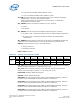
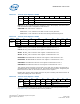
Table 140. FPGA Register Overview
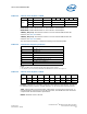
Table 139. FPGA Register Legend
Symbol Description
U Unchanged (stay unchanged after reset)
X Not Defined
NU Not Used
80h POST Code
81h Extended POST Code (16-bit write only)
A00h FPGA Version
A01h Debug LED Control
A02h FWUM Control (manufacturing use only)
A03h Reserved
A04h Development Features
A05-A07h Reserved
A08h Telecom Clock Register 0: Configuration
A09h Telecom Clock Register 1: Configuration
A0Ah Telecom Clock Register 2: Configuration & Status
A0Bh Telecom Clock Register 3: Configuration
A0Ch Telecom Clock Register 4: Reset and Test Modes
A0Dh Telecom Clock Register 5: PLD Version
A0Eh Telecom Clock Register 6: Alarms
A0Fh Telecom Clock Register 7: Interrupt Number
A10-A1Fh Reserved