
user manual

Intel NetStructure
®
MPCBL0010 Single Board Computer
October 2006 Technical Product Specification
Order Number: 304120 173
Telecom Clock—MPCBL0010 SBC
DRVCLK3B: Enables MLVDS buffer to drive CLK3B to the backplane
DRVCLK3A: Enables MLVDS buffer to drive CLK3A to the backplane
TXREF1_SEL[2..0]: Transmission reference clock for AdvancedMC module B2
selection (see Table 145 below).
TXREF0_SEL[2..0]: Transmission reference clock for AdvancedMC module B1
selection (see Table 145 below).
The transmission frequency is selected according to the following table:
Notes:
† 8kHz or 16 MHz can be selected by bit 8K_16M in telecom clock register 1.
‡ One frequency can be selected by bits E3DS3 and E3DS3OC3 in telecom clock register 0.
IRQTST: Interrupt test. The state of this bit is OR’d with the real interrupt. This bit is
for software testing. Ignore in normal operation. A "1" asserts the interrupt request.
TEST: Ignores IPMC and shelf manager authorization. Use this bit for testing only. In
normal operation, leave this bit set to “0”. Otherwise, the MPCBL0010 SBC will not be
compliant with the AdvancedTCA specification.
RESET: Hardware reset of the PLL.
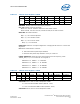
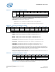
Table 144. Telecom Clock Register 3 0A0Bh
AddressAction D7 D6 D5D4D3D2D1D0
0xA0B
Read DRVCLK3B DRVCLK3A TXREF1_SEL[2..0] TXREF0_SEL[2..0]
Write DRVCLK3B DRVCLK3A TXREF1_SEL[2..0] TXREF0_SEL[2..0]
Reset 0 0 000 000
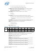
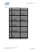
Table 145. Transmission Frequency Selection
TXREFx_SEL[2..0] Transmission Clock Frequency
000 1.544 MHz (T1, J1)
001 2.048 MHz (E1)
010 4.096 MHz (E1)
011 6.312 MHz (J2)
100 8.192 MHz (E1)
101 8 kHz / 16.384 MHz
†
(E1, T1, J1, J2)
110 19.44 MHz (OC3, 12/STM-1, 4)
111 34.368 / 44.736 MHz
‡
(E3, T3) or 8.592 / 11.184 MHz
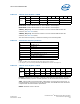
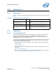
Table 146. Telecom Clock Register 4 0A0Ch
Addres
s
Action D7 D6 D5 D4 D3 D2 D1 D0
0xA0C
Read NU NU NU NU NU IRQTST RESET TEST
WriteNUNUNUNUNUIRQTSTRESETTEST
ResetXXXXX010