
Laptop User Manual

4-10 Intel® PXA26x Processor Family Developer’s Manual
System Integration Unit
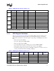
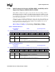
Table 4-6. GPDR0 Bit Definitions
Physical Address
0x40E0_000C
GPDR0 System Integration Unit
Bit
31 30 29 28 27 26 25 24 23 22 21 20 19 18 17 16 15 14 13 12 11 10 9 8 7 6 5 4 3 2 1 0
PD31
PD30
PD29
PD28
PD27
PD26
PD25
PD24
PD23
PD22
PD21
PD20
PD19
PD18
PD17
PD16
PD15
PD14
PD13
PD12
PD11
PD10
PD9
PD8
PD7
PD6
PD5
PD4
PD3
PD2
PD1
PD0
Reset 0 0 0 0 0 0 0 0 0 0 0 0 0 0 0 0 0 0 0 0 0 0 0 0 0 0 0 0 0 0 0 0
Bits Name Description
<31:0> PD[x]
GPIO Pin ‘x’ Direction (where x = 0 to 31).
0 – Pin configured as an input.
1 – Pin configured as an output
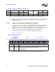
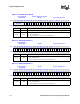
Table 4-7. GPDR1 Bit Definitions
Physical Address
0x40E0_0010
GPDR1 System Integration Unit
Bit
31 30 29 28 27 26 25 24 23 22 21 20 19 18 17 16 15 14 13 12 11 10 9 8 7 6 5 4 3 2 1 0
PD63
PD62
PD61
PD60
PD59
PD58
PD57
PD56
PD55
PD54
PD53
PD52
PD51
PD50
PD49
PD48
PD47
PD46
PD45
PD44
PD43
PD42
PD41
PD40
PD39
PD38
PD37
PD36
PD35
PD34
PD33
PD32
Reset 0 0 0 0 0 0 0 0 0 0 0 0 0 0 0 0 0 0 0 0 0 0 0 0 0 0 0 0 0 0 0 0
Bits Name Description
<31:0> PD[x]
GPIO Pin ‘x’ Direction (where x = 32 to 63).
0 – Pin configured as an input.
1 – Pin configured as an output.
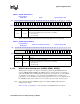
Table 4-8. GPDR2 Register Bitmap
Physical Address
0x40E0_0014
GPIO Pin Direction Register2
(GPDR2)
System Integration Unit
Bit
31 30 29 28 27 26 25 24 23 22 21 20 19 18 17 16 15 14 13 12 11 10 9 8 7 6 5 4 3 2 1 0
Reserved
PD89
PD88
PD87
PD86
PD85
PD84
PD83
PD82
PD81
PD80
PD79
PD78
PD77
PD76
PD75
PD74
PD73
PD72
PD71
PD70
PD69
PD68
PD67
PD66
PD65
PD64
Reset 0 0 0 0 0 0 0 0 0 0 0 0 0 0 0 0 0 0 0 0 0 0 0 0 0 0 0 0 0 0 0 0
Bits Name Description
<31:26> — Reserved
<25:22> PD[x]
GPIO Pin ‘x’ Direction (where x = 86 to 89).
0 – Pin configured as an output
1 – Pin configured as an input
<21:0> PD[x]
GPIO Pin ‘x’ Direction (where x = 64 to 85).
0 – Pin configured as an input.
1 – Pin configured as an output