
Laptop User Manual

Intel® PXA26x Processor Family Developer’s Manual 2-9
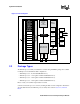
System Architecture
• Sleep mode – low power mode that does not save state but keeps I/Os powered. While the
RTC, power manager, and clock module states are saved, coprocessor 14 is not.
Note: In low power modes, ensure that input pins are not floating and output pins are not driven by an
external device in conflict with how the processor is driving that pin. In either case, the system
draws excess current. Current draw that varies in sleep mode or varies greatly between parts is
typically a sign of floating pins.
Section 3.4, “Resets and Power Modes” describes the modes in detail.
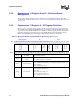
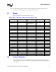
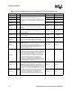
2.12 Pin List
Some of the processor pins can be connected to multiple signals. The signal connected to the pin is
determined by the GPIO Alternate Function Select Registers (GAFRn_m). Some signals can be
connected to multiple pins. The signal must be routed to only one pin by using the GAFRn_m
registers. Because this is true, some pins are listed twice, once in each unit that can use the pin.
Table 2-6 describes the PXA26x processor family pins.
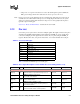
Table 2-5. Processor Pin Types
Type Function
IC CMOS input
OC CMOS output
OCZ CMOS output, Hi-Z
ICOCZ CMOS bidirectional, Hi-Z
IA Analog input
OA Analog output
IAOA Analog bidirectional
SUP Supply pin (either VCC or VSS)
Table 2-6. Pin & Signal Descriptions for the PXA26x Processor Family (Sheet 1 of 12)
Pin Name Type Signal Descriptions Reset State Sleep State
Memory Controller Pins
MA[25:0] OCZ
MEMORY ADDRESS BUS (output):
Signals the address requested for memory accesses.
Driven Low Driven Low
MD[15:0] ICOCZ
MEMORY DATA BUS (input/output):
Lower 16 bits of the data bus.
Hi-Z Driven Low
MD[31:16] ICOCZ
MEMORY DATA BUS (input/output):
Used for 32-bit memories.
Hi-Z Driven Low
nOE OCZ
MEMORY OUTPUT ENABLE (output):
Connect to the output enables of memory devices to
control data bus drivers.
Driven High Note [4]
nWE OCZ
MEMORY WRITE ENABLE (output):
Connect to the write enables of memory devices.
Driven High Note [4]