
Technical Product Specification

Connector/Header Locations and Pin-outs Intel® Server System SC5650HCBRP TPS
Revision 1.2
Intel order number E81443-002
158
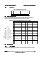
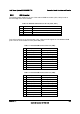
Pin Name Pin
Name
35 GND 36 PE_ICH10_SAS_SW_RXP2
37 PE_ICH10_SAS_SW_RXN2 38 GND
39 GND 40 PE_ICH10_SAS_SW_RXP3
41 PE_ICH10_SAS_SW_RXN3 42 GND
43 GND 44 CLK_100M_SAS_DP
45 CLK_100M_SAS_DN 46 GND
47 GND 48 P3V3
49 P3V3 50 P3V3
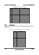
8.5.5 Serial Port Connectors
The server board provides one external DB9 Serial A port (J8A1) and one internal 9-pin Serial B
header (J1B1). The following tables define the pin-outs.
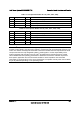
Table 108. External DB9 Serial A Port Pin-out (J8A1)
Pin Signal Name Description
1 SPA_DCD DCD (carrier detect)
2 SPA_SIN_L RXD (receive data)
3 SPA_SOUT_N TXD (Transmit data)
4 SPA_DTR DTR (Data terminal ready)
5 GND Ground
6 SPA_DSR DSR (data set ready)
7 SPA_RTS RTS (request to send)
8 SPA_CTS CTS (clear to send)
9 SPA_RI RI (Ring Indicate)
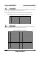
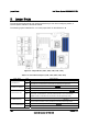
Table 109. Internal 9-pin Serial B Header Pin-out (J1B1)
Pin Signal Name
Description
1 SPB_DCD DCD (carrier detect)
2 SPB_DSR DSR (data set ready)
3 SPB_SIN_L RXD (receive data)
4 SPB_RTS RTS (request to send)
5 SPB_SOUT_N TXD (Transmit data)
6 SPB_CTS CTS (clear to send)
7 SPB_DTR DTR (Data terminal ready)
8 SPB_RI RI (Ring indicate)
9 SPB_EN_N Enable