
Dual Intel Xeon Processor Voltage Regulator Down (VRD) Design Guidelines

Dual Intel
®
Xeon™ Processor Voltage Regulator Down (VRD) Guidelines
16
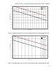
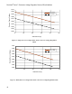
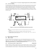
ensure that the supply voltage on the system board does not go outside of regulation
requirements during times of transient load on the VRD.
2.3 Control Inputs REQUIRED
2.3.1 Output Enable—(OUTEN)
The VR should accept an open-collector, open-drain, open-switch-to-ground, low-voltage TTL
or low-voltage CMOS signal to enable the output. The input should have a pull-up resistor
between 1 kΩ and 10 kΩ to 3.3V. The maximum low-input voltage is 0.8V; the minimum high-
input voltage is 1.7V. When disabled, the VR should not sink or source current. When Output
Enable is pulled low during the shutdown process, the VR should not exceed its previous voltage
level regardless of the VID setting.
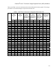
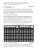
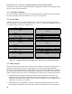
2.3.2 Voltage Identification—(VID[4:0])
The VR must accept five input lines to set the nominal voltage as defined by the table below.
Five processor pins (VID[4:0]) will have either an open-ground combination (Intel Xeon
Processor) or open-drain driver outputs (Intel Xeon Processor with 512 KByte L2 cache and
Low Voltage Intel Xeon processor). When all five VID inputs are high (11111), such as when
no processor is installed, the VR should disable its output.
The maximum low-input voltage is 0.8V; the minimum high-input voltage is 1.7V. Each VID
input should have a 1 kΩ ± 10% pull-up resistor to 3.3V ± 5%. Board designers using other
values should check them against data sheets for the VR components and the processor.
Table 4 – Voltage Identification (VID)
Processor Pins (0 = low, 1 = high) Vcc Processor Pins (0 = low, 1 = high) Vcc
VID4 VID3 VID2 VID1 VID0 (VDC) VID4 VID3 VID2 VID1 VID0 (VDC)
1 1 1 1 1 Off 01111 1.475
1 1 1 1 0 1.1 0 1 1 1 0 1.5
1 1 1 0 1 1.125 0 1 1 0 1 1.525
1 1 1 0 0 1.15 0 1 1 0 0 1.55
1 1 0 1 1 1.175 0 1 0 1 1 1.575
1 1 0 1 0 1.2 0 1 0 1 0 1.6
1 1 0 0 1 1.225 0 1 0 0 1 1.625
1 1 0 0 0 1.250 0 1 0 0 0 1.65
1 0 1 1 1 1.275 0 0 1 1 1 1.675
1 0 1 1 0 1.3 0 0 1 1 0 1.7
1 0 1 0 1 1.325 0 0 1 0 1 1.725
1 0 1 0 0 1.35 0 0 1 0 0 1.75
1 0 0 1 1 1.375 0 0 0 1 1 1.775
1 0 0 1 0 1.4 0 0 0 1 0 1.8
1 0 0 0 1 1.425 0 0 0 0 1 1.825
1 0 0 0 0 1.45 0 0 0 0 0 1.85
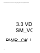
2.4 Power Good Output (PWRGD) REQUIRED
The VRD should provide an open collector or equivalent Power Good signal consistent with
TTL DC levels. This signal should transition to the open (>100kΩ) state within 10ms of the
output voltage stabilizing within the range specified in Section 2.1.1. The signal should be in the