
Voltage Regulator Module (VRM) and Enterprise Voltage Regulator-Down (EVRD) 10.1 Design Guidelines


Voltage Regulator Module (VRM) and Enterprise Voltage 21
Regulator-Down (EVRD) 10.1 Design Guidelines
Control Signals
3.3 Differential Remote Sense (VO_SEN±) - REQUIRED
The PWM controller should include differential sense inputs to compensate for an output voltage
offset of <300 mV in the power distribution path. This common mode voltage is expected to occur
due to transient currents and parasitic inductances and is not expected to be caused by parasitic
resistances. The remote sense lines should draw no more than 10m A, to minimize offset errors.
3.4 Load Line Select (LL0, LL1) - REQUIRED
Control signals LL0 and LL1 form a 2-bit load line selection and are used to configure the
VRM/EVRD to supply the proper load line for the processor. These control signals, LL0 and LL1,
are generated from a board management chip to set the load line for the processor. LL0 and LL1 are
open-collector/drain or equivalent signal. Table 3-4 shows the LL0 and LL1 pins specification and
Table 2-1 shows equations in how to obtain V
MAX
and V
MIN
based on LL0 and LL1 bit code. It is
EXPECTED that the pull-up resistor will be located on the baseboard and will not be integrated
into the VRM.
§
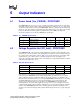
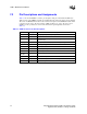
Table 3-4. LL0, LL1 Specifications
Symbol Parameter Min Max Units
I
OL
Output Low Current 0 4 mA
V
IH
Input Voltage High 0.8 3.465 V
V
IL
Input Voltage Low 0 0.4 V