
Datasheet


4
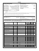
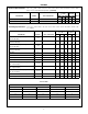
Absolute Maximum Ratings Thermal Information (Typical, Note 1)
Supply Voltage, V
DD
and V
CC
. . . . . . . . . . . . . . . . . . . -0.3V to 16V
Logic I/O Voltages . . . . . . . . . . . . . . . . . . . . . . . -0.3V to V
DD
+0.3V
Voltage on AHS, BHS. . . . -6.0V (Transient) to 80V (25
o
C to 125
o
C)
Voltage on AHS, BHS. . . -6.0V (Transient) to 70V (-55
o
C to 125
o
C)
Voltage on ALS, BLS . . . . . . . -2.0V (Transient) to +2.0V (Transient)
Voltage on AHB, BHB. . . . . . . V
AHS, BHS
-0.3V to V
AHS, BHS
+16V
Voltage on ALO, BLO . . . . . . . . . . . . V
ALS, BLS
-0.3V to V
CC
+0.3V
Voltage on AHO, BHO . . . . . .V
AHS, BHS
-0.3V to V
AHB, BHB
+0.3V
Input Current, HDEL and LDEL . . . . . . . . . . . . . . . . . . -5mA to 0mA
Phase Slew Rate . . . . . . . . . . . . . . . . . . . . . . . . . . . . . . . . . . 20V/ns
NOTE: All voltages are relative to pin 4, V
SS
, unless otherwise
specified.
Storage Temperature Range. . . . . . . . . . . . . . . . . . .-65
o
C to 150
o
C
Operating Max. Junction Temperature . . . . . . . . . . . . . . . . . . 125
o
C
Lead Temperature (Soldering 10s) . . . . . . . . . . . . . . . . . . . . . 300
o
C
(For SOIC - Lead Tips Only)
Thermal Resistance, Junction-Ambient
SOIC Package. . . . . . . . . . . . . . . . . . . . . . . . . . . . . . . . . .85
o
C/W
DIP Package . . . . . . . . . . . . . . . . . . . . . . . . . . . . . . . . . . .75
o
C/W
CAUTION: Stresses above those listed in “Absolute Maximum Ratings” may cause permanent damage to the device. This is a stress only rating and operation
of the device at these or any other conditions above those indicated in the operational sections of this specification is not implied.
NOTE:
1. θ
JA
is measured with the component mounted on an evaluation PC board in free air.
Operating Conditions
Supply Voltage, V
DD
and V
CC
. . . . . . . . . . . . . . . . . . . +6V to +15V
Voltage on ALS, BLS . . . . . . . . . . . . . . . . . . . . . . . . . -1.0V to +1.0V
Voltage on AHB, BHB . . . . . . . . V
AHS, BHS
+5V to V
AHS, BHS
+15V
Input Current, HDEL and LDEL. . . . . . . . . . . . . . . . -500µA to -50µA
Operating Ambient Temperature Range . . . . . . . . . . .-40
o
C to 85
o
C
Electrical Specifications V
DD
= V
CC
= V
AHB
= V
BHB
= 12V, V
SS
= V
ALS
= V
BLS
= V
AHS
= V
BHS
= 0V, R
HDEL
= R
LDEL
= 100K
and T
A
= 25
o
C, Unless Otherwise Specified
PARAMETER SYMBOL TEST CONDITIONS
T
J
= 25
o
C
T
JS
= -40
o
C
TO 125
o
C
UNITSMIN TYP MAX MIN MAX
SUPPLY CURRENTS AND CHARGE PUMPS
V
DD
Quiescent Current I
DD
All Inputs = 0V 7 9 11 6 12 mA
V
DD
Operating Current I
DDO
Outputs Switching f = 500kHz 8 9.5 12 7 13 mA
V
CC
Quiescent Current I
CC
All Inputs = 0V, I
ALO
= I
BLO
= 0 - 0.1 10 - 20 µA
V
CC
Operating Current I
CCO
f = 500kHz, No Load 1 1.25 2.0 0.8 3 mA
AHB, BHB Quiescent Current -
Qpump Output Current
I
AHB
, I
BHB
All Inputs = 0V, I
AHO
= I
BHO
= 0
V
DD
= V
CC
= V
AHB
= V
BHB
= 10V
-50 -30 -15 -60 -10 µA
AHB, BHB Operating Current I
AHBO
, I
BHBO
f = 500kHz, No Load 0.5 0.9 1.3 0.4 1.7 mA
AHS, BHS, AHB, BHB Leakage Current I
HLK
V
AHS
= V
BHS
= V
AHB
= V
BHB
= 95V - 0.02 1.0 - 10 µA
AHB-AHS, BHB-BHS Qpump
Output Voltage
V
AHB
-V
AHS
V
BHB
-V
BHS
I
AHB
= I
AHB
= 0, No Load 11.5 12.6 14.0 10.5 14.5 V
INPUT PINS: ALI, BLI, AHI, BHI, AND DIS
Low Level Input Voltage V
IL
Full Operating Conditions - - 1.0 - 0.8 V
High Level Input Voltage V
IH
Full Operating Conditions 2.5 - - 2.7 - V
Input Voltage Hysteresis -35---mV
Low Level Input Current I
IL
V
IN
= 0V, Full Operating Conditions -130 -100 -75 -135 -65 µA
High Level Input Current I
IH
V
IN
= 5V, Full Operating Conditions -1 - +1 -10 +10 µA
TURN-ON DELAY PINS: LDEL AND HDEL
LDEL, HDEL Voltage V
HDEL,
V
LDEL
I
HDEL
= I
LDEL
= -100µA 4.9 5.1 5.3 4.8 5.4 V
GATE DRIVER OUTPUT PINS: ALO, BLO, AHO, AND BHO
Low Level Output Voltage V
OL
I
OUT
= 100mA 0.7 0.85 1.0 0.5 1.1 V
High Level Output Voltage V
CC
-V
OH
I
OUT
= -100mA 0.8 .95 1.1 0.5 1.2 V
HIP4081