
Datasheet


6
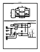
Pin Descriptions
PIN
NUMBER SYMBOL DESCRIPTION
1 BHB B High-side Bootstrap supply. External bootstrap diode and capacitor are required. Connect cathode of boot-
strap diode and positive side of bootstrap capacitor to this pin. Internal charge pump supplies 30µA out of this
pin to maintain bootstrap supply. Internal circuitry clamps the bootstrap supply to approximately 12.8V.
2 BHI B High-side Input. Logic level input that controls BHO driver (Pin 20). BLI (Pin 5) high level input overrides BHI
high level input to prevent half-bridge shoot-through, see Truth Table. DIS (Pin 3) high level input overrides BHI
high level input. The pin can be driven by signal levels of 0V to 15V (no greater than V
DD
). An internal 100µA
pull-up to V
DD
will hold BHI high, so no connection is required if high-side and low-side outputs are to be con-
trolled by the low-side input.
3 DIS Disable input. Logic level input that when taken high sets all four outputs low. DIS high overrides all other inputs.
When DIS is taken low the outputs are controlled by the other inputs. The pin can be driven by signal levels of
0V to 15V (no greater than V
DD
). An internal 100µA pull-up to V
DD
will hold DIS high if this pin is not driven.
4V
SS
Chip negative supply, generally will be ground.
5 BLI B Low-side Input. Logic level input that controls BLO driver (Pin 18). If BHI (Pin 2) is driven high or not connected
externally then BLI controls both BLO and BHO drivers, with dead time set by delay currents at HDEL and LDEL
(Pin 8 and 9). DIS (Pin 3) high level input overrides BLI high level input. The pin can be driven by signal levels
of 0V to 15V (no greater than V
DD
). An internal 100µA pull-up to V
DD
will hold BLI high if this pin is not driven.
6 ALI A Low-side Input. Logic level input that controls ALO driver (Pin 13). If AHI (Pin 7) is driven high or not connected
externally then ALI controls both ALO and AHO drivers, with dead time set by delay currents at HDEL and LDEL
(Pin 8 and 9). DIS (Pin 3) high level input overrides ALI high level input. The pin can be driven by signal levels
of 0V to 15V (no greater than V
DD
). An internal 100µA pull-up to V
DD
will hold ALI high if this pin is not driven.
7 AHI A High-side Input. Logic level input that controls AHO driver (Pin 11). ALI (Pin 6) high level input overrides AHI
high level input to prevent half-bridge shoot-through, see Truth Table. DIS (Pin 3) high level input overrides AHI
high level input. The pin can be driven by signal levels of 0V to 15V (no greater than V
DD
). An internal 100µA
pull-up to V
DD
will hold AHI high, so no connection is required if high-side and low-side outputs are to be con-
trolled by the low-side input.
8 HDEL High-side turn-on DELay. Connect resistor from this pin to V
SS
to set timing current that defines the turn-on de-
lay of both high-side drivers. The low-side drivers turn-off with no adjustable delay, so the HDEL resistor guar-
antees no shoot-through by delaying the turn-on of the high-side drivers. HDEL reference voltage is
approximately 5.1V.
9 LDEL Low-side turn-on DELay. Connect resistor from this pin to V
SS
to set timing current that defines the turn-on delay
of both low-side drivers. The high-side drivers turn-off with no adjustable delay, so the LDEL resistor guarantees
no shoot-through by delaying the turn-on of the low-side drivers. LDEL reference voltage is approximately 5.1V.
10 AHB A High-side Bootstrap supply. External bootstrap diode and capacitor are required. Connect cathode of boot-
strap diode and positive side of bootstrap capacitor to this pin. Internal charge pump supplies 30µA out of this
pin to maintain bootstrap supply. Internal circuitry clamps the bootstrap supply to approximately 12.8V.
11 AHO A High-side Output. Connect to gate of A High-side power MOSFET.
12 AHS A High-side Source connection. Connect to source of A High-side power MOSFET. Connect negative side of
bootstrap capacitor to this pin.
13 ALO A Low-side Output. Connect to gate of A Low-side power MOSFET.
14 ALS A Low-side Source connection. Connect to source of A Low-side power MOSFET.
15 V
CC
Positive supply to gate drivers. Must be same potential as V
DD
(Pin 16). Connect to anodes of two bootstrap
diodes.
16 V
DD
Positive supply to lower gate drivers. Must be same potential as V
CC
(Pin 15). De-couple this pin to V
SS
(Pin 4).
17 BLS B Low-side Source connection. Connect to source of B Low-side power MOSFET.
18 BLO B Low-side Output. Connect to gate of B Low-side power MOSFET.
19 BHS B High-side Source connection. Connect to source of B High-side power MOSFET. Connect negative side of
bootstrap capacitor to this pin.
20 BHO B High-side Output. Connect to gate of B High-side power MOSFET.
HIP4081