MX919B COMMUNICATION SEMICONDUCTORS DATA BULLETIN 4-Level FSK Modem Data Pump PRELIMINARY INFORMATION Features Applications • 4-Level Root Raised Cosine FSK Modulation • Wireless Data Terminals • Half Duplex, 4800 to 19.
4-Level FSK Modem Data Pump Page 2 of 47 MX919B PRELIMINARY INFORMATION CONTENTS Section Page 1. Block Diagram ............................................................................................................... 6 2. Signal List ...................................................................................................................... 7 3. External Components ................................................................................................... 8 4.
4-Level FSK Modem Data Pump Page 3 of 47 MX919B PRELIMINARY INFORMATION 4.5.2.17 T4S: Transmit 4 Symbols ............................................................................................... 20 4.5.2.18 RESET: Stop any current action .................................................................................... 20 4.5.2.19 Task Timing .................................................................................................................... 20 4.5.2.20 RRC Filter Delay...........
-Level FSK Modem Data Pump Page 4 of 47 MX919B PRELIMINARY INFORMATION 6. Performance Specification ......................................................................................... 41 6.1 Electrical Performance..................................................................................................... 41 6.1.1 Absolute Maximum Ratings .................................................................................................. 41 6.1.2 Operating Limits.........................
4-Level FSK Modem Data Pump Page 5 of 47 MX919B PRELIMINARY INFORMATION Figures Figure Page Figure 1: Block Diagram ..................................................................................................................................... 6 Figure 2: Recommended External Components ................................................................................................ 8 Figure 3: Typical Modem µC connections ...........................................................................
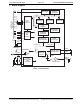
4-Level FSK Modem Data Pump Page 6 of 47 MX919B PRELIMINARY INFORMATION 1.
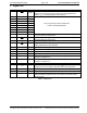
4-Level FSK Modem Data Pump Page 7 of 47 MX919B PRELIMINARY INFORMATION 2. Signal List Pin No.
4-Level FSK Modem Data Pump Page 8 of 47 MX919B PRELIMINARY INFORMATION 3.
4-Level FSK Modem Data Pump Page 9 of 47 MX919B PRELIMINARY INFORMATION 4. General Description 4.1 4.1.1 Description of Blocks Data Bus Buffers Eight bi-directional 3-state logic level buffers between the modem's internal registers and the host µC's data bus lines. 4.1.
4-Level FSK Modem Data Pump Page 10 of 47 MX919B PRELIMINARY INFORMATION 4.1.10 Rx Input Amp This amplifier allows the received signal input to the modem to be set to the optimum level by suitable selection of the external components R1 and R2. The value of R1 should be calculated to give 0.2 x VDD voltsP-P at the RXAMPOUT pin for a received '...+3 +3 -3 -3 ...' sequence. A capacitor may be placed in series with R1 if ac coupling of the received signal is desired (see Section 5.
4-Level FSK Modem Data Pump Page 11 of 47 MX919B PRELIMINARY INFORMATION 0 -5 -10 dB -15 -20 -25 -30 0 0.1 0.2 0.3 0.4 0.5 Frequency / Bit Rate Figure 5: RRC Filter Frequency Response vs. Bit Rate (including the external RC filter R4/C5) 0 -5 -10 dB -15 -20 -25 -30 0 0.2 0.4 0.6 0.8 1.0 Frequency / Symbol Rate Figure 6: RRC Filter Frequency Response vs. Symbol Rate (including the external RC filter R4/C5) 4.1.
4-Level FSK Modem Data Pump Page 12 of 47 MX919B PRELIMINARY INFORMATION 4.1.13 Rx Level/Clock Extraction These circuits, which operate only in receive mode, derive a symbol rate clock from the received signal and measure the received signal amplitude and DC offset. This information is then used to extract the received 4level symbols and also to provide an input to the received Data Quality measuring circuit. The external capacitors C6 and C7 form part of the received signal level measuring circuit.
4-Level FSK Modem Data Pump 4.3 Page 13 of 47 MX919B PRELIMINARY INFORMATION Binary to Symbol Translation Although the over-air signal, and therefore the signals at the modem TXOUT and RXIN pins, consists of 4level symbols, the raw data passing between the modem and the µC is in binary form. Translation between binary data and the 4-level symbols is done in one of two ways, depending on the task being performed. 1. Direct way: (simplest form) - converts between 2 binary bits and a single symbol.
4-Level FSK Modem Data Pump 4.4 Page 14 of 47 MX919B PRELIMINARY INFORMATION Frame Structure Figure 7 shows how an over-air message frame may be constructed from a sequence of: a Symbol Sync pattern (preamble), a Frame Sync pattern, and one or more 'Header', 'Intermediate' or 'Last' blocks. Byte 0 1 2 3 4 5 6 7 8 9 10 11 µC binary data stored in MX919B data block memory configured as header, intermediate, or last block by MX919B task being executed.
4-Level FSK Modem Data Pump A B C Page 15 of 47 MX919B PRELIMINARY INFORMATION SYMBOL SYNC FRAME SYNC 'HEADER' BLOCKS SYMBOL SYNC FRAME SYNC 'INTERMEDIATE' BLOCKS SYMBOL SYNC FRAME SYNC 'INTERMEDIATE' BLOCKS 'LAST' BLOCK Figure 8: Alternative Frame Structures The MX919B performs the entire block formatting and de-formatting required to convert data between µC binary form and Over-Air as shown in Figure 7. 4.
4-Level FSK Modem Data Pump 4.5.2.1 Page 16 of 47 MX919B PRELIMINARY INFORMATION Command Register B7: AQSC - Acquire Symbol Clock This bit has no effect in transmit mode. In receive mode, when a byte with the AQSC bit set to '1' is written to the Command Register, and TASK is not set to RESET, it initiates an automatic sequence designed to achieve symbol timing synchronization with the received signal as quickly as possible.
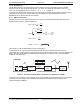
4-Level FSK Modem Data Pump Page 17 of 47 Data from µC to Block Buffer MX919B PRELIMINARY INFORMATION Task 1 data Task 2 data Task from µC to Command Register BFREE Bit of Status Register IRQ Bit of Status Register IRQ Output (IRQEN = '1') TXOUT Signal from Task 1 from Task 2 Figure 9: Transmit Task Overlapping When the modem is in receive mode, the µC should wait until the BFREE bit of the Status Register is '1', then write the desired task to the Command Register.
4-Level FSK Modem Data Pump Page 18 of 47 MX919B PRELIMINARY INFORMATION MX919B Modem Tasks: B2 0 0 0 0 1 1 1 1 B1 0 0 1 1 0 0 1 1 4.5.2.
4-Level FSK Modem Data Pump Page 19 of 47 MX919B PRELIMINARY INFORMATION 4.5.2.12 R4S: Read 4 Symbols This task causes the modem to read the next 4 symbols and translate them directly (without de-interleaving or FEC) to an 8-bit byte which is placed into the Data Block Buffer. The BFREE and IRQ bits of the Status Register are then set to '1' to indicate that the µC may read the data byte from the Data Block Buffer and write the next task to the Command Register.
4-Level FSK Modem Data Pump Page 20 of 47 MX919B PRELIMINARY INFORMATION 4.5.2.15 TIB: Transmit Intermediate Block This task takes 12 bytes of data from the Data Block Buffer, updates the 4-byte CRC2 checksum for inclusion in the 'Last' block, translates the 12 data bytes to 4-level symbols (with FEC), interleaves the symbols, and transmits the result as a formatted 'Intermediate' Block.
4-Level FSK Modem Data Pump Data to Data Block Buffer Page 21 of 47 1 Task to Command Register MX919B PRELIMINARY INFORMATION 3 2 1 2 t4 3 t4 t4 IBEMPTY Bit BFREE Bit t2 t2 t2 t3 t3 t3 t1 Symbols to RRC Filter from Task 3 from Task 2 from Task 1 Modem Tx Output Figure 11: Transmit Task Timing Diagram Modem Rx Input Symbols to De-Interleave Circuit for Task 1 for Task 2 for Task 3 t5 t5 t5 1 2 Data from Data Block Buffer Task to Command Register t6 1 t6 2 t7 t6 t7 3
4-Level FSK Modem Data Pump 4.5.3 Page 22 of 47 MX919B PRELIMINARY INFORMATION Control Register This 8-bit write-only register controls the modem's symbol rate, the response times of the receive clock extraction, signal level measurement circuits, and the Frame Sync pattern recognition tolerance to inexact matches. Control Register 7 6 CKDIV 4.5.3.
4-Level FSK Modem Data Pump 4.5.3.3 Page 23 of 47 MX919B PRELIMINARY INFORMATION Control Register B3, B2: LEVRES - Level Measurement Modes These two bits have no effect in transmit mode. In receive mode they set the 'normal' or 'steady state' operating mode of the Rx signal amplitude and DC offset measuring and tracking circuits.
4-Level FSK Modem Data Pump Page 24 of 47 MX919B PRELIMINARY INFORMATION The 'Hold' setting disables the feedback loop of the PLL which continues to run at a rate determined only by the actual crystal frequency and the setting of the Control Register CKDIV bits, not the PLL's operating frequency immediately prior to the 'Hold' setting. 4.5.4 Mode Register The contents of this 8-bit write only register control the basic operating modes of the modem: Mode Register 7 6 5 IRQEN INVSYM Tx/Rx 4.5.4.
4-Level FSK Modem Data Pump 4.5.4.4 Page 25 of 47 MX919B PRELIMINARY INFORMATION Mode Register B4: RXEYE - Show Rx Eye This bit should normally be set to '0'. Setting it to '1' when the modem is in receive mode configures the modem for a special test mode, in which the input of the Tx output buffer is connected to the Rx Symbol/Clock extraction circuit at a point which carries the equalized receive signal.
4-Level FSK Modem Data Pump 4.5.5 Page 26 of 47 MX919B PRELIMINARY INFORMATION Status Register This register may be read by the µC to determine the current state of the modem. Status Register 7 IRQ 4.5.5.
4-Level FSK Modem Data Pump 4.5.5.5 Page 27 of 47 MX919B PRELIMINARY INFORMATION Status Register B3: CRCERR - CRC Checksum Error In receive mode, this bit will be updated at the end of a SFSH, RHB or RILB task to reflect the result of the receive CRC check. '0' indicates that the CRC was received correctly, '1' indicates an error. Note: This bit should be ignored when an 'Intermediate' block (which does not have an integral CRC) is received.
4-Level FSK Modem Data Pump 4.6.1.2 Page 28 of 47 MX919B PRELIMINARY INFORMATION CRC2 This is a thirty-two-bit CRC check code contained in bytes 8 to 11 of the 'Last' Block, which provides error detection coverage for the combined Intermediate Blocks and Last Block of a message.
4-Level FSK Modem Data Pump Page 29 of 47 MX919B PRELIMINARY INFORMATION Figure 17: Tx Signal Eye TXIMP = 0 Figure 18: Tx Signal Eye TXIMP = 1 Note: Setting TXIMP to '1' affects the Tx output signal level as shown in Section 6.1.3 and the table below. Nominal Voltage difference between continuous ‘+3’ and continuous ‘-3’ symbol outputs Nominal VP-P for continuous ‘+3+3-3-3…’ symbol pattern. ©2001 MX•COM, INC. www.mxcom.
4-Level FSK Modem Data Pump Page 30 of 47 MX919B PRELIMINARY INFORMATION 5. Application 5.1 Transmit Frame Example The operations needed to transmit a single Frame consisting of Symbol and Frame Sync sequences, and one each Header, Intermediate and Last blocks are provided below: 1. Ensure that the Control Register has been loaded with a suitable CKDIV value, that the IRQEN and TX/RX bits of the Mode Register are '1', the RXEYE and PSAVE bits are '0', and the INVSYM bit is set appropriately. 2.
4-Level FSK Modem Data Pump Page 31 of 47 MX919B PRELIMINARY INFORMATION START Ensure that the Control Register has been loaded with a suitable CKDIV value Set µC variable 'IBLOCKS' to the number of Intermediate blocks to be transmitted Ensure that the Mode Register IRQEN, PSAVE and RXEYE bits are '0', the TX/RX bit is '1', and the INVSYM bit is set appropriately Set µC variable 'STATE' to 0 Set the Mode Register IRQEN bit to '1' Write a RESET task to the Command Register Enable µC's MX919B Tx Inter
4-Level FSK Modem Data Pump Page 32 of 47 MX919B PRELIMINARY INFORMATION Value of µC variable 'STATE' on entry to IRQ routine and corresponding MX919B's actions: 0: Symbol Sync pattern being transmitted, load Frame Sync pattern & T24S task. 1: Frame Sync pattern being transmitted, load Header Block bytes and THB task. 2: Header or Intermmediate Block being transmitted, load Intermediate or Last Block bytes & TIB or TLB task. 3: Last block being transmitted, . ignore this interrupt.
4-Level FSK Modem Data Pump 5.2 Page 33 of 47 MX919B PRELIMINARY INFORMATION Receive Frame Example The operations needed to receive a single Frame consisting of Symbol and Frame Sync sequences and one each Header, Intermediate and Last blocks are shown below; 1. Ensure that the Control Register has been loaded with suitable CKDIV, FSTOL, LEVRES and PLLBW values, and that the IRQEN bit of the Mode Register is '1', the TX /RX PSAVE, and RXEYE bits are '0', and the INVSYM bit is set appropriately. 2.
4-Level FSK Modem Data Pump Page 34 of 47 MX919B PRELIMINARY INFORMATION START Ensure that the Control Register has been loaded with suitable CKDIV, FSTOL, LEVRES and PLLBW values Wait until the received carrier has been present for at least 8 symbol times Ensure that the Mode Register IRQEN, PSAVE, RXEYE and TX/RX bits are '0', and the INVSYM bit is set appropriately Set µC variable 'STATE' to 0 Write a RESET task to the Command Register Set the Mode Register IRQEN bit to '1' Read the Status Register
4-Level FSK Modem Data Pump Page 35 of 47 START MX919B PRELIMINARY INFORMATION Value of µC variable 'STATE' on entry to IRQ routine and corresponding MX919B's actions: ( IRQ line goes low ) 0 : Frame Sync has been recognized and Header block received, read out data and load RILB task. Read Status Register 1 : Intermediate block has been received, read out data and load RILB task. IRQ bit = 1 ? 2 : Last block has been received, read out data and finish.
4-Level FSK Modem Data Pump 5.3 Page 36 of 47 MX919B PRELIMINARY INFORMATION Clock Extraction and Level Measurement Systems 5.3.1 Supported Types of Systems The MX919B is intended for use in systems where: 1. The Symbol Sync pattern is transmitted immediately on start-up of the transmitter, before the first Frame Sync pattern (see Figure 23). 2.
4-Level FSK Modem Data Pump 5.3.4 Page 37 of 47 MX919B PRELIMINARY INFORMATION Automatic Acquisition Functions Setting the AQSC and AQLEV bits to '1' triggers the modem's automatic Symbol Clock Extraction and Level Measurement acquisition sequences, which are designed to measure the received symbol timing, amplitude, and DC offset as quickly as possible before switching to accurate - but slower - measurement modes.
4-Level FSK Modem Data Pump Page 38 of 47 MX919B PRELIMINARY INFORMATION 2. Any ac coupling at the receive input will transform any step in the voltage at the discriminator output to a slowly decaying pulse which can confuse the modem's level measuring circuits.
4-Level FSK Modem Data Pump 5.5 Page 39 of 47 MX919B PRELIMINARY INFORMATION Radio Performance The maximum data rate that can be transmitted over a radio channel using these modems depends on: • RF channel spacing. • Allowable adjacent channel interference. • Symbol rate. • Peak carrier deviation (modulation index). • Tx and Rx reference oscillator accuracy. • Modulator and demodulator linearity. • Receiver IF filter frequency and phase characteristics. • Use of error correction techniques.
4-Level FSK Modem Data Pump 5.6 Page 40 of 47 MX919B PRELIMINARY INFORMATION Received Signal Quality Monitor In applications where the modem has to monitor a long transmission containing a number of concatenated Frames, it is recommended that the controlling software include a function which regularly checks that the modem is still receiving a good data signal and triggers a re-acquisition and possibly changes to another channel if a problem is encountered.
4-Level FSK Modem Data Pump Page 41 of 47 MX919B PRELIMINARY INFORMATION 6. Performance Specification 6.1 6.1.1 Electrical Performance Absolute Maximum Ratings Exceeding these maximum ratings can result in damage to the device.
4-Level FSK Modem Data Pump 6.1.3 Page 42 of 47 MX919B PRELIMINARY INFORMATION Operating Characteristics For the following conditions unless otherwise specified: Xtal Frequency = 4.9152MHz, Symbol Rate = 4800 symbols/sec, Noise Bandwidth = 0 to 9600Hz, VDD = 5.0V @ TAMB = 25°C Notes DC Parameters IDD IDD (VDD = 3.3V) IDD (Powersave Mode) IDD (Powersave Mode, VDD = 3.
4-Level FSK Modem Data Pump 6.1.4 Page 43 of 47 MX919B PRELIMINARY INFORMATION Timing µC Parallel Interface Timings (see Figure 28 ) tACSL Address valid to CS low time tAH tCSH Address hold time tCSHI CS high time tCSRWL Notes Min. 0 Typ. Max.
4-Level FSK Modem Data Pump Page 44 of 47 MX919B PRELIMINARY INFORMATION WRITE CYCLE (DATA TO MODEM) tAH ADDRESS A0, A1 ADDRESS VALID tACSL tCSH tCSHI CS tWL WR tRHCSL tCSRWL RD tDSW tDHW DATA D0 to D7 (1 byte) DATA VALID READ CYCLE (DATA FROM MODEM) tAH ADDRESS A0, A1 ADDRESS VALID tACSL tCSH CS tCSHI tWHCSL WR tCSRWL tRL RD tRX tRARL DATA D0 to D7 (1 byte) tDHR DATA VALID tRACL Figure 28: µC Parallel Interface Timings ©2001 MX•COM, INC. www.mxcom.
4-Level FSK Modem Data Pump 6.1.
4-Level FSK Modem Data Pump 6.2 Page 46 of 47 MX919B PRELIMINARY INFORMATION Packaging Package Tolerances A Z B ALTERNATIVE PIN LOCATION MARKING E W L T PIN 1 X Y C K H P J DIM. A B C E H J K L P T W X Y Z MIN. TYP. MAX. 0.613 (15.57) 0.299 (7.59) 0.105 (2.67) 0.419 (10.64) 0.020 (0.51) 0.020 (0.51) 0.046 (1.17) 0.597 (15.16) 0.286 (7.26) 0.093 (2.36) 0.390 (9.90) 0.003 (0.08) 0.013 (0.33) 0.036 (0.91) 0.050 (1.27) 0.016 (0.41) 0.050 (1.27) 0.0125 (0.32) 0.009 (0.
4-Level FSK Modem Data Pump Page 47 of 47 E B C Package Tolerances K DIM. A B C D E F G H J K P T W Y Y DA J W W H T PIN 1 MX919B PRELIMINARY INFORMATION P G MIN. TYP. MAX. 0.409 (10.40) 0.380 (9.61) 0.409 (10.40) 0.380 (9.61) 0.146 (3.70) 0.128 (3.25) 0.417 (10.60) 0.435 (11.05) 0.417 (10.60) 0.435 (11.05) 0.250 (6.35) 0.250 (6.35) 0.023 (0.58) 0.018 (0.45) 0.022 (0.55) 0.047 (1.19) 0.048 (1.22) 0.049 (1.24) 0.051 (1.30) 0.006 (0.152) 0.009 (0.