
Data Sheet


4-Level FSK Modem Data Pump Page 5 of 47 MX919B PRELIMINARY INFORMATION
©2001 MX•COM, INC. www.mxcom.com Tele: 800 638 5577 336 744 5050 Fax: 336 744 5054 Doc. # 20480170.003
4800 Bethania Station Road, Winston-Salem, NC 27105-1201 USA All trademarks and service marks are held by their respective companies.
Figures
Figure Page
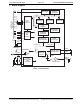
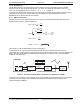
Figure 1: Block Diagram ..................................................................................................................................... 6
Figure 2: Recommended External Components ................................................................................................ 8
Figure 3: Typical Modem µC connections .......................................................................................................... 9
Figure 4: Translation of Binary Data to Filtered 4-Level Symbols in Tx Mode................................................. 10
Figure 5: RRC Filter Frequency Response vs. Bit Rate (including the external RC filter R4/C5).................... 11
Figure 6: RRC Filter Frequency Response vs. Symbol Rate (including the external RC filter R4/C5)............ 11
Figure 7: Over-Air Signal Format ..................................................................................................................... 14
Figure 8: Alternative Frame Structures ............................................................................................................ 15
Figure 9: Transmit Task Overlapping ............................................................................................................... 17
Figure 10: Receive Task Overlapping .............................................................................................................. 17
Figure 11: Transmit Task Timing Diagram ....................................................................................................... 21
Figure 12: Receive Task Timing Diagram ........................................................................................................ 21
Figure 13: RRC Low Pass Filter Delay............................................................................................................. 21
Figure 14: Ideal 'RXEYE' Signal....................................................................................................................... 25
Figure 15: Typical Data Quality Reading vs S/N.............................................................................................. 27
Figure 16: Input Signal to RRC Filter in Tx Mode for TXIMP = 0 and 1...........................................................28
Figure 17: Tx Signal Eye TXIMP = 0................................................................................................................ 29
Figure 18: Tx Signal Eye TXIMP = 1................................................................................................................ 29
Figure 19: Transmit Frame Example Flowchart, Main Program ......................................................................31
Figure 20: Tx Interrupt Service Routine ........................................................................................................... 32
Figure 21: Receive Frame Example Flowchart, Main Program ........................................................................34
Figure 22: Rx Interrupt Service routine ............................................................................................................ 35
Figure 23: Acquisition Sequence Timing.......................................................................................................... 36
Figure 24: Effect of AC Coupling on BER (without FEC) ................................................................................. 37
Figure 25: Decay Time - AC Coupling.............................................................................................................. 38
Figure 26: Typical Connections between Radio and MX919B......................................................................... 39
Figure 27: Received Signal Quality Monitor Flowchart .................................................................................... 40
Figure 28: µC Parallel Interface Timings.......................................................................................................... 44
Figure 29: Typical Bit Error Rate With and Without FEC ................................................................................. 45
Figure 30: 24-pin SOIC Mechanical Outline: Order as part no. MX919BDW ................................................. 46
Figure 31: 24-pin SSOP Mechanical Outline: Order as part no. MX919BDS ................................................. 46
Figure 32: 24-pin PLCC Mechanical Outline : Order as part no. MX919BLH ................................................. 47
Figure 33: 24-pin PDIP Mechanical Outline: Order as part no. MX919BP ..................................................... 47