
Data Sheet


4-Level FSK Modem Data Pump Page 8 of 47 MX919B PRELIMINARY INFORMATION
©2001 MX•COM, INC. www.mxcom.com Tele: 800 638 5577 336 744 5050 Fax: 336 744 5054 Doc. # 20480170.003
4800 Bethania Station Road, Winston-Salem, NC 27105-1201 USA All trademarks and service marks are held by their respective companies.
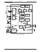
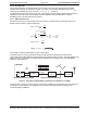
3. External Components
DOC1
DOC2
V
DD
V
DD
V
SS
V
BIAS
RXIN
From Rx FM
Discriminator
To Tx Frequency
Modulator
RXAMPOUT
R2
R4
R1
µCONTROLLER INTERFACE
MX919B
TXOUT
C7
C5
C3
C4
R3
X1
C6
C8
C2
D7
D6
D5
D4
D3
D2
D1
D0
A0
A1
A1
A0
XTAL/CLOCK
XTAL/CLOCK
1
2
3
4
5
6
8
9
10
11
12
13
14
7
24
23
22
21
20
19
18
17
17
16
16
15
IRQ
XTAL
XTAL
RD
WR
CS
CS
C1
Figure 2: Recommended External Components
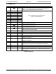
Component Notes Value Tolerance Component Notes Value Tolerance
R1 3
±20%
C4 3
±20%
R2
100kΩ ±5%
C5 4
±5%
R3
1MΩ ±20%
C6 5
±20%
R4
100kΩ ±5%
C7 5
±20%
C1 0.1µF
±20%
C8 4
±5%
C2 0.1µF
±20%
C3 3
±20%
X1 2,3
Table 2: Recommended External Components
Recommended External Component Notes:
1. See Section 4.1.10.
2. For best results, a crystal oscillator design should drive the clock inverter input with signal levels of at
least 40% of V
DD
, peak to peak. Tuning fork crystals generally cannot meet this requirement. To obtain
crystal oscillator design assistance, consult your crystal manufacturer.
3. The values used for C3 and C4 should be suitable for the frequency of the crystal X1. As a guide, values
(including stray capacitance) of 33pF at 1MHz falling to 18pF at 10MHz will generally prove suitable.
Crystal frequency tolerances are discussed in Section 4.5.3.4.
4. Values C5 and C8 should be equal to 750,000 / symbol rate, e.g.
5. Values C6 and C7 should be equal to 50,000 / symbol rate, e.g.
Symbol Rate C5 and C8 Symbol Rate C6 and C7
2400 symbols/second 330pF 2400 symbols/second 0.022µF
4800 symbols/second 150pF 4800 symbols/second 0.01µF
9600 symbols/second 82pF 9600 symbols/second 4700pF