
User Manual
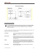
Table Of Contents

SECTION 1: THEORY OF OPERATION
IP4HPVGPS-MRFCCRpt.doc Page 5
IP4HPV Mobile Radio Section Descriptions
The IP4HPV Mobile Radio works within a frequency range of 506 to 512 MHz and requires a 1/4-
wavelength antenna.
This section provides detailed descriptions of each of the sections within the IP4HPV Mobile Radio.
Refer to Appendix A to view the IP4HPV Mobile Radio Circuit Board Diagram.
Microcontroller
The microcontroller (U30) is a major component of the radio as it manages the operation of the radio. It
also controls the operation of the modem, and determines which receiver provides a better signal from a
given transmission. It provides transmit time-out protection in the event a fault causes the radio to halt in
the transmit mode. It utilizes a reduced instruction set computer (RISC) architecture which provides low
power operation and a powerful instruction set. Other features include a watchdog timer, serial universal
asynchronous receiver/transmitter (UART), two 8-bit timers, and 2 KB of electrically erasable
programmable read only memory (EEPROM) storage.
NOTE
: The EEPROM Random Access Memory (RAM) stores the setup data entered by the
technician even if there is a loss of power.
Support circuitry
The support circuitry consists of the following:
A Supervisor Control Chip (U25) provides power-on reset.
The clock controls microcontroller operation and is generated by crystal Y3 and a Pierce oscillator
circuit (inside the U30-microcontroller).
The latch (U28) decodes low order address bits (A0-A7) from the address/data bits (AD0-AD7). It is
controlled by Address Latch Enable (ALE) output of U30 and the bits are used by the modem.
A 512Kx8 Static RAM Chip (U31) provides temporary storage of the radio’s configuration data
facilitating the technician with access to make changes.
Control logic is also an important part in the microcontroller section. The RAM chip select (RAMCS*)
and modem chip select (MODEMCS*) command lines are created by U26A, U27BCD, and U44ABC.
These gates decode four (4) high order address bits (A11-A15). The RAM is addressed by five (5)
memory addresses (MA14-MA18) bits decoded by U26D, U27A, and U24. This logic decodes port
address bits (PA14-PA18) to produce memory address bits (MA14-MA18) for the RAM chip.
Input/Output
Input/output components convert serial and handshake data from the modem section to RS232 levels,
and vice-versa. Chip U22 is an RS232 transmitter and receiver. It converts data in 5-volt logic form to
data in +/-12-volt form, as required by the RS232 standard. A charge pump power supply on the chip
converts the +5-volt DC logic power on pin 26 to the +12-volt and –12-volt levels required. Capacitors
C106-C109 generate these voltages by a charge pump. These values determine the operating voltages.