
User Manual
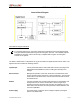
Table Of Contents

SECTION 1: THEORY OF OPERATION
IP4HPVGPS-MRFCCRpt.doc Page 8
The lower op amp (U70C) amplifies the signal from the low pass filter and applies it to the VCO via the
VCOMOD output. Pot RV1 and RV2 are used to adjust maximum deviation.
Injection Synthesizer
The dual synthesizer chip (U38) is the major contributor of the injection synthesizer. This device contains
the key components of a phase locked loop (PLL), including a prescaler, programmable divider, and
phase detector. The selected frequencies are loaded into U38 as a clocked serial bit stream via the PLL
DATA, PLL CLOCK and PLL ENABLE signals.
Frequency stability is determined by a temperature-compensated crystal oscillator module (VCTCXO)
(Y5) at a frequency stability of 1 PPM from –30C to +60C. This device has an input (REFMOD) that
accepts transmit modulation and voltage from a RX FREQ ADJUST pot. The pot allows the receiver to
be fine-tuned to the exact operating frequency.
Two (2) voltage control oscillators (VCO) are formed by integrated low-noise oscillators with buffered
outputs (U39 and U40) and associated circuitry. The VCO’s generate receiver and transmit injection
signals. The receiver control voltage is generated by the phase detector output (PDOUT) of U38 driving a
loop filter consisting of R111, R112, C185, C186, C42, R133, and C213. It integrates the pulses that
normally appear on PDOUT into a smooth DC control signal for U40. The output of U40 is split by U63
leading to outputs RXINJ1 and RXINJ2. A second output of U40 is returned to the synthesizer FIN input
via RXFB. This completes the loop signal path.
The transmitter control voltage is generated by the phase detector output (PDOUT-L) of U38 driving a
loop filter consisting of transmitter R135, R118, C195, C196, and C214. It integrates the pulses that
normally appear on PDOUT-L into a smooth DC control signal for U39. Upon transmit, the analog signal
from the modem and transmit processing circuitry is applied to the U39 tuning circuit at CR6. The output
of U39 is the TXINJ signal. A second output of U39 returns to the synthesizer F-IN input via TXFB.
Transmitter/TR Switch
The transmitter section consists of a driver amplifier (U36) and a final power amplifier (U35). To transmit,
5-volt power is applied to the KEYPWR line. PA12V line is also powered up. This causes power
amplifier (U35) to boost the RF power to the desired level. Up to 40 watts are available from the
transmitter. Harmonic suppression is provided by C233, L43, and L44.
Power and Analog Ground
These sections consist of the power supplies and transmit control circuitry. Power from the vehicle’s
battery appears at VBATT. Diode D1 protects the voltage regulators by clamping any transient spikes on
the supply line. Such spikes typically occur while the engine is started. The supply line powers a series
of voltage regulators and the transmitter control circuitry, as follows:
Voltage regulator U46 provides 8-volt power for most other sections in the radio.
Voltage regulator U21 powers the transmit driver and T/R switch diodes as controlled by the
microcontroller.
Voltage regulator VR2 provides a low noise 3.3-volt source for the radio electronics.
In the transmit control circuitry, to transmit, the microcontroller makes TXKEYOUT* high. Forcing the P-
channel device to conduct, applying 12-volts via PA12V to the transmitter power amplifier bias pins.