
Datasheet

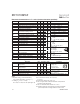


IRF1010NPbF
www.irf.com 7
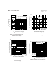
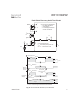
Peak Diode Recovery dv/dt Test Circuit
P.W.
Period
di/dt
Diode Recovery
dv/dt
Ripple ≤ 5%
Body Diode Forward Drop
Re-Applied
Voltage
Reverse
Recovery
Current
Body Diode Forward
Current
V
GS
=10V
V
DD
I
SD
Driver Gate Drive
D.U.T. I
SD
Waveform
D.U.T. V
DS
Waveform
Inductor Curent
D =
P. W .
Period
+
-
+
+
+
-
-
-
R
G
V
DD
• dv/dt controlled by R
G
• I
SD
controlled by Duty Factor "D"
• D.U.T. - Device Under Test
D.U.T*
Circuit Layout Considerations
• Low Stray Inductance
• Ground Plane
• Low Leakage Inductance
Current Transformer
* Reverse Polarity of D.U.T for P-Channel
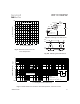
V
GS
[ ]
[ ]
*** V
GS
= 5.0V for Logic Level and 3V Drive Devices
[ ] ***
Fig 14. For N-channel HEXFET
®
power MOSFETs