
Datasheet


Features
• Floating channel designed for bootstrap operation
• Fully operational to +600 V
• Tolerant to negative transient voltage, dV/dt
immune
• Gate drive supply range from 10 V to 20 V
• Undervoltage lockout for both channels
• 3.3 V logic compatible
• Separate logic supply range from 3.3 V to 20 V
• Logic and power ground +/- 5 V offset
• CMOS Schmitt-triggered inputs with pull-down
• Cycle by cycle edge-triggered shutdown logic
• Matched propagation delay for both channels
• Outputs in phase with inputs
Product Summary
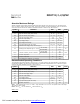
V
OFFSET
600 V max.
I
O
+/- 200 mA / 440 mA
V
OUT
10 V - 20 V
t
on/off
(typ.) 135 ns & 105 ns
Delay Matching 30 ns
www.irf.com 1
Data Sheet No. PD60251
IRS2112
(
-1,-2,S
)
PbF
Description
The IRS2112 is a high voltage, high speed power
M
OSFET and IGBT driver with
independent high- and
low-side referenced output channels. Proprietary HVIC
and latch immune CMOS technologies enable rug-
gedized monolithic construction. Logic inputs are com-
patible with standard CMOS or LSTTL outputs, down
to 3.3 V logic. The output drivers feature a high pulse
current buffer stage designed for minimum driver
cross-conduction. Propagation delays are matched
to simplify use in high frequency applications. The
floating channel can be used to drive an N-channel power MOSFET or IGBT in the high-side configuration
which operates up to 600 V.
(Refer to Lead Assignments for correct pin configuration). This diagram shows electrical connections only. Please
refer to our Application Notes and DesignTips for proper circuit board layout.
Typical Connection
HIN
up to 600 V
TO
LOAD
V
DD
V
B
V
S
HO
LO
COM
HIN
LIN
V
SS
SD
V
CC
LIN
V
DD
SD
V
SS
V
CC
Packages
16-Lead SOIC
IRS2112S
14-Lead PDIP
(w/o lead 4)
IRS2112-1
14-Lead PDIP
IRS2112
16-Lead PDIP
(w/o leads 4 & 5)
IRS2112-2
HIGH AND LOW SIDE DRIVER
• RoHS compliant