
Specifications


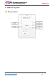


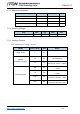
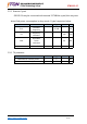
Table Of Contents
- Version:
- Overview
- Brief
- Features
- Application
- Hardware System
- Function block
- PIN assignment
- PIN description
- Schematic diagram
- Electronic parameter
- Basic parameter
- Maximum parameter
- Working Voltage
- Working Current
- External Crystal
- TX parameter
- Dimensions
- Mechanical dimensions
- Layout reference dimensions
- Process parameters
- Recommended temperature curve
- Package information
- Please be noticed following information and instru
- FCC Certification Requirement:

深圳市中易腾达科技股份有限公司
iTON Technology Corp. STB1132-25
http://www.sziton.com/
7
/
16
13
ADC2
I/O
14
DIO13/Wake-up
When module in sleep,
lower level this PIN to wake
up module
Pull down duration≥50ms
15
DIO12
I/O
16
GND
POWER
17
DIO0
I/0
18
UART_RX
UART RX PIN
19
UART_TX
UART TX PIN
20
DIO4
I/O
21
DIO5
I/O
22
DIO3/Mode_N
Mode select PIN
H: Data mode
L: Command mode
Default: H
23
DIO2
I/O
24
DIO1/UART_TX_
IND
Time delay control PIN for
sending data from module
to MCU
Default Close
Can use command to set up
the time delay
25
GND
POWER
2.4 Schematic diagram