
Datasheet


IXD_604
R02 www.clare.com 3
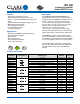
1 Specifications
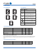
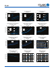
1.1 Pin Configurations
1.2 Pin Definitions
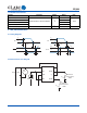
1.3 Absolute Maximum Ratings
Absolute maximum electrical ratings are at 25°C
Absolute maximum ratings are stress ratings. Stresses in excess of these ratings can cause permanent damage to the device.
Functional operation of the device at conditions beyond those indicated in the operational sections of this data sheet is not
implied.
1.4 Recommended Operating Conditions
IXDD604PI/SI/SIA
ENA
INA
GND
INB
ENB
OUTA
V
CC
OUTB
1
4
3
2
8
5
6
7
A
B
IXDF604PI/SI/SIA
NC
INA
GND
INB
NC
OUTA
V
CC
OUTB
1
4
3
2
8
5
6
7
A
B
IXDI604PI/SI/SIA
NC
INA
GND
INB
NC
OUTA
V
CC
OUTB
1
4
3
2
8
5
6
7
A
B
IXDN604PI/SI/SIA
NC
INA
GND
INB
NC
OUTA
V
CC
OUTB
1
4
3
2
8
5
6
7
A
B
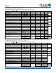
IXDD604D2
ENA
INA
INB
ENB
OUTA
GND
V
CC
OUTB
A
1
4
3
2
8
5
6
7
B
Pin Name Description
INA Channel A Logic Input
INB Channel B Logic Input
ENA
Channel A Enable Input -
Drive pin low to disable Channel A and force
Channel A Output to a high impedance state
ENB
Channel B Enable Input -
Drive pin low to disable Channel A and force
Channel A Output to a high impedance state
OUTA
OUTA
Channel A Output - Sources or sinks current to
turn-on or turn-off a discrete MOSFET or IGBT
OUTB
OUTB
Channel B Output - Sources or sinks current to
turn-on or turn-off a discrete MOSFET or IGBT
V
CC
Supply Voltage - Provides power to the device
GND
Ground - Common ground reference for the
device
Parameter Symbol Minimum Maximum Units
Supply Voltage
V
CC
-0.3 40 V
Input Voltage
V
INx
, V
ENx
-5
V
CC
+0.3
V
Output Current
I
OUT
-±4A
Junction Temperature
T
J
-55 +150
°C
Storage Temperature
T
STG
-65 +150 °C
Parameter Symbol Minimum Maximum Units
Supply Voltage
V
CC
4.5 35 V
Operating Temperature Range
T
A
-40 +125 °C