
Datasheet


IXD_609
12 www.clare.com R02
5.4.3 Tape & Reel Information for SI and SIA Packages
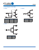
5.4.4 YI (5-Pin TO-263)
NOTES:
1. A
0
& B
0
measured at 0.3mm above base of pocket.
2. 10 pitches cumulative tol. ± 0.2mm
3. ( ) Reference dimensions only.
4. Unless otherwise specified, all dimensions in millimeters.
K
0
=2.30 ± 0.10
B
0
=5.20 ± 0.10
R0.50 TYP
8.00 ± 0.10
2.00 ± 0.10
4.00 ± 0.10 See Note #2
12.00 ± 0.30
5.50 ± 0.10
1.75 ± 0.10
∅1.50 (MIN)
∅1.55 ± 0.05
1.80 ± 0.10
(3.40)
0.30 ± 0.05
(70º)
A
0
=6.40 ± 0.10
(4.70)
(1.20)
A
A
B
B
SECTION A-A
SECTION B-B
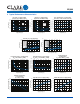
Embossment
Embossed Carrier
Top Cover
Tape Thickness
0.102 MAX.
(0.004 MAX.)
330.2 DIA.
(13.00 DIA.)
DIMENSIONS
mm MIN / mm MAX
(inches MIN / inches / MAX)
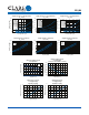
NOTES:
1. All metal surfaces are solder-plated except trimmed area.
2. Short lead of No. 3 is optional to IXYS.
3. No. 3 lead is connected to No. 6 lead (bottom heat sink) internally.
8.80 / 9.50
(0.346 / 0.374)
14.80 / 15.80
(0.583 / 0.622)
9.65 / 10.30
(0.380 / 0.406)
1.70 BSC
(0.067 BSC)
1 2 3 4 5
0.60 / 0.99
(0.024 / 0.039)
1.00 / 1.40
(0.039 / 0.055)
4.20 / 4.80
(0.165 / 0.189)
1.20 / 1.40
(0.047 / 0.055)
0.40 / 0.70
(0.016 / 0.028)
2.24 / 2.84
(0.088 / 0.112)
2.10 / 2.70
(0.083 / 0.106)
0º - 3º
6.60 / 7.20
(0.260 / 0.283)
7.50 / 8.20
(0.295 / 0.323)
1.20 / 1.70
(0.047 / 0.067)
6
Optional
3.85
(0.152)
3.65
(0.144)
6.35
(0.250)
1.05
(0.041)
1.70
(0.067)
10.40
(0.409)
9.15
(0.360)
Recommended PCB Pattern