
Datasheet

IXFA10N80P IXFP10N80P
IXFQ10N80P IXFH10N80P
IXYS Reserves the Right to Change Limits, Test Conditions, and Dimensions.
Note 1. Pulse test, t ≤ 300 μs, duty cycle d ≤ 2 %
IXYS MOSFETs and IGBTs are covered 4,835,592 4,931,844 5,049,961 5,237,481 6,162,665 6,404,065 B1 6,683,344 6,727,585 7,005,734 B2 7,157,338B2
by one or more of the following U.S. patents: 4,850,072 5,017,508 5,063,307 5,381,025 6,259,123 B1 6,534,343 6,710,405 B2 6,759,692 7,063,975 B2
4,881,106 5,034,796 5,187,117 5,486,715 6,306,728 B1 6,583,505 6,710,463 6,771,478 B2 7,071,537
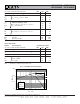
Symbol Test Conditions Characteristic Values
(T
J
= 25°C, Unless Otherwise Specified) Min. Typ. Max
g
fs
V
DS
= 20V, I
D
= 0.5 • I
D25
, Note 1 7 11 S
C
iss
2050 pF
C
oss
V
GS
= 0V, V
DS
= 25V, f = 1MHz 172 pF
C
rss
16 pF
t
d(on)
21 ns
t
r
22 ns
t
d(off)
62 ns
t
f
22 ns
Q
g(on)
40 nC
Q
gs
V
GS
= 10V, V
DS
= 0.5 • V
DSS
, I
D
= 0.5 • I
D25
12 nC
Q
gd
14 nC
R
thJC
0.42 °C/W
R
thCS
(TO-220) 0.50 °C/W
R
thCS
(TO-247 & TO-3P) 0.25 °C/W
Source-Drain Diode
Symbol Test Conditions Characteristic Values
(T
J
= 25°C, Unless Otherwise Specified) Min. Typ. Max
I
S
V
GS
= 0V 10 A
I
SM
Repetitive, Pulse WidthLlimited by T
JM
30 A
V
SD
I
F
= I
S
, V
GS
= 0V, Note 1 1.5 V
t
rr
200 250 ns
I
RM
3.0 A
Q
RM
0.6 μC
I
F
= 10A, V
GS
= 0V
-di/dt = 100A/μs
V
R
= 100V
Resistive Switching Times
V
GS
= 10V, V
DS
= 0.5 • V
DSS
, I
D
= 0.5 • I
D25
R
G
= 5Ω (External)
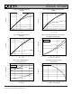
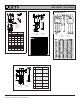
Fig. 1. Forward-Bias Safe Operating Area
0.1
1.0
10.0
100.0
10 100 1000
V
DS
- Volts
I
D
-
Amperes
T
J
= 150ºC
T
C
= 25ºC
Single Pulse
1m s
100µs
25µs