
Datasheet

© 2000 IXYS All rights reserved
2 - 4
Symbol Test Conditions Characteristic Values
I
RRM
, I
DRM
T
VJ
= T
VJM
; V
R
= V
RRM
; V
D
= V
DRM
10 mA
V
T
, V
F
I
T
, I
F
= 300 A; T
VJ
= 25°C 1.25 V
V
T0
For power-loss calculations only (T
VJ
= 125°C) 0.88 V
r
T
1.15 mW
V
GT
V
D
= 6 V; T
VJ
= 25°C 2.5 V
T
VJ
= -40°C 2.6 V
I
GT
V
D
= 6 V; T
VJ
= 25°C 150 mA
T
VJ
= -40°C 200 mA
V
GD
T
VJ
= T
VJM
;V
D
= 2/3 V
DRM
0.2 V
I
GD
10 mA
I
L
T
VJ
= 25°C; t
P
= 30 ms; V
D
= 6 V 300 mA
I
G
= 0.5 A; di
G
/dt = 0.5 A/ms
I
H
T
VJ
= 25°C; V
D
= 6 V; R
GK
= ¥ 200 mA
t
gd
T
VJ
= 25°C; V
D
= 1/2 V
DRM
2 ms
I
G
= 0.5 A; di
G
/dt = 0.5 A/ms
t
q
T
VJ
= T
VJM
; I
T
= 300 A, t
P
= 200 ms; -di/dt = 10 A/ms typ. 150 ms
V
R
= 100 V; dv/dt = 20 V/ms; V
D
= 2/3 V
DRM
Q
S
T
VJ
= T
VJM
; I
T
, I
F
= 300 A, -di/dt = 50 A/ms 550 mC
I
RM
235 A
R
thJC
per thyristor/diode; DC current 0.155 K/W
per module other values 0.0775 K/W
R
thJK
per thyristor/diode; DC current see Fig. 8/9 0.225 K/W
per module 0.1125 K/W
d
S
Creepage distance on surface 12.7 mm
d
A
Strike distance through air 9.6 mm
a Maximum allowable acceleration 50 m/s
2
Optional accessories for modules
Keyed gate/cathode twin plugs with wire length = 350 mm, gate = yellow, cathode = red
Type ZY 180L (L = Left for pin pair 4/5) UL 758, style 1385,
Type ZY 180R (R = right for pin pair 6/7) CSA class 5851, guide 460-1-1
Dimensions in mm (1 mm = 0.0394")
MCC Version 1 MCD Version 1
MCC162
MCD162
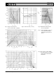
Fig. 1 Gate trigger characteristics
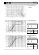
Fig. 2 Gate trigger delay time