
3 CCD RGB Color Camera CV-M91 Operation Manual

CV-M91
- 7 -
6. Functions and Operations
The different camera modes and functions can be set by switches and jumpers. Some functions
like RGB setup and white clip can only be changed via RS-232C.
Function names within “ “ are names used in camera control tool.
6.1. Input/Output of Signals
6.1.1. Input/output of HD/VD
In the default setting the camera will accept external HD/VD signals on pin 6 and 7 of the 12 pin
Hirose connector. If external HD/VD is applied, the camera will synchronize to it. If no external
sync signals are applied, the camera will operate with its internal x-tal controlled sync.
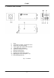
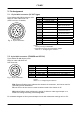
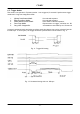
The time requirements to the relation between VD and HD are shown in fig. 10.
The input is TTL level as factory setting. It can be 75 Ohm terminated by an internal switch.
Internal HD/VD signals can be output on pin 6 and 7 by internal jumper settings. The output is
TTL level from a 75-Ohm source. In trigger modes a VD pulse will only be output after an
external trigger pulse.
Refer to “7. Configuring the Camera.”
To use this mode:
Set function on PK8407: JP305 s, JP306 o for ext. VD input. Factory default.
JP308 s, JP309 o for ext. HD input. Factory default.
SW301-1(HD), SW301-2(VD) to OFF for TTL level. Factory default.
SW301-1(HD), SW301-2(VD) to ON for 75 Ω termination
JP305 o, JP306 s for int. VD output
JP308 o, JP309 s for int. HD output
Input/output: Ext. VD in or int. VD out on pin 7 on 12-pin connector.
Ext. HD in or int. HD out on pin 6 on 12-pin connector.
If only a composite VS signal is available, it is possible to enable an internal sync separator to
separate HD and VD from the composite signal.
To use this mode:
Set jumper on PK8407: JP312 s, JP313 o, JP315 o, JP318 s, JP319 o for HD/VD input. Default.
JP312 o, JP313 s, JP315 s, JP318 o JP319 s for comp. VS input.
Input Ext. VS (1Vpp ±30%) on pin 7 on 12 pin connector.
Important notes on using this mode.
• External sync system should follow the camera scanning system
• Requirements to HD/VD phase is shown in fig. 10
Fig. 10. Ext. HD and VD phase conditions.