
Microprocessor User's Manual

164 Rabbit 3000 Microprocessor
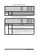
12.1 Serial Port Register Layout
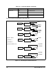
Figure 12-2 shows a functional block diagram of a serial port. Each serial port has a data
register, a control register and a status register. Writing to the data register starts transmis-
sion. The least significant bit (LSB) is always transmitted first. This is true for both asyc-
nchronous and synchronous communication. If the write is performed to an alternate data
register address, the extra address bit or 9th bit (8th bit if 7 data bits) is sent. When data
bits have been received, they are read from the data register (LSB first). The control regis-
ter is used to set the transmit and receive parameters. The status register may be tested to
check on the operation of the serial port.
Figure 12-2. Functional Block Diagram of a Serial Port
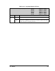
Bit 0 1 2 3 4 5 6 7 stop
Rx serial data in
Tx serial data out
Read Data Write Data
Input Shift Reg
Data In Reg
Data Out Reg
Start Bit
0 1 1 0 1 0 1 1
Transmitting 0x0D6
Stop Bit
Tx
Start Bit
Bit 0 1 2 3 4 5 6 7 A stop
0 1 1 0 1 0 1 1
Transmitting 0x0D6
Stop Bit
Tx
9th bit
with 9th bit zero
Signals Shown at Microprocessor Tx Pin
fifo ports E, F only
(4-bytes deep)
fifo ports E, F only
(4-bytes deep)
output shift
reg
9th bit
zero
9th bit
one
alternate data out
registers
address register
long stop register
LSB First
LSB First