
Microprocessor User's Manual


64 Rabbit 3000 Microprocessor
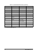
5.4 Bus Timing
The external bus has essentially the same timing for memory cycles or I/O cycles. A mem-
ory cycle begins with the chip select and the address lines. One clock later, the output
enable is asserted for a read. The output data and the write enable are asserted for a write.
Figure 5-6. Bus Timing Read and Write
In some cases, the timing shown in Figure 5-6 may be prefixed by a false memory access
during the first clock, which is followed by the access sequence shown in Figure 5-6. In
this case, the address and often the chip select will change values after one clock and
assume the final values for the memory to be actually accessed. Output enable and write
enable are always delayed by one clock from the time the final, stable address and chip
select are enabled. Normally the false memory access attempts to start another instruction
access cycle, which is aborted after one clock when the processor realizes that a read data
or write data bus cycle is needed. The user should not attempt a design that uses the chip
select or a memory address as a clock or state changing signal without taking this into con-
sideration.
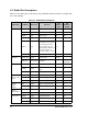
Address (20 for memory, 16 for I/O)
T1 Tw
T2
/IOCSn or /CSn
Data for read
valid
/OEn or /IORD and /BUFEN (/BUFEN rd or wr)
Data for write 3-s drive starts at end of T1
/WEn or /IOWR
Notes:
Read may have no wait states.
Write cycles and I/O read cycles have at least 1 wait state. Clock
may be asymmetric if clock doubler used. I/O chip select available
on port E as option.