Jiangsu JWT Electronics Shares CO.,Ltd. WIRELESS TRANSCEIVER MODULE SPEC Client: Product name:2.4G Transceiver module Part number:JRF 201103-1_V1.1 Edition:V1.
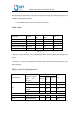
Jiangsu JWT Electronics Shares CO.,Ltd. Catalog One.Product picture ............................................................................................................. 4 Two.Summarize......................................................................................................................... 4 limit value .......................................................................................................................... 5 Major electrical parameters .............................
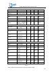
Jiangsu JWT Electronics Shares CO.,Ltd. 1、Launch timing .................................................................................................. 25 2、Receive sequence .......................................................................................... 27 3、Automatic reply and automatic retransmission .......................................... 28 4、CRC16 verification .......................................................................................
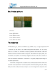
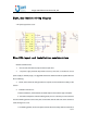
Jiangsu JWT Electronics Shares CO.,Ltd. One.Product picture Picture 1-1 Illustrate: Row 1: JWT LOGO Row 2: Product name Row 3: Product model Row 4: Date Year Week Two.Summarize JRF JRF201103-1_V1.1 module use JD0069C* chip, JD0069C chip is a single integrated wireless transceiver chip that works in the 2.4GHz world general ISM spectrum.
Jiangsu JWT Electronics Shares CO.,Ltd. the advantages of small volume, low power consumption and high sensitivity of transceiver, it is suitable for batch patch production. * * The JD0069C chip silk screen is RC2516S, hereby explain. limit value value Maximum value Unit Top -10 50 ℃ Storage Temperature Tstor -20 70 ℃ working voltage VDD 1.9 3.
Jiangsu JWT Electronics Shares CO.,Ltd. PLL_stable FCH 1M PLL Settling time 150 us code rate 1 Mbps Channel spacing 1 MHz maximum output 8 dBm 0 dBm Emission pattern index PRF PRF PRFC PBW1 power Typical output Output Power Range Carrier -24 modulated 1 20dB Mbps(1Mbps) 8 dBm 1.1 MHz Receiving mode index RXSENS2 receiving sensitivity (0.
Jiangsu JWT Electronics Shares CO.,Ltd. Three.Product characteristics low power consumption When work is in launch mode(Transmitted power 0.
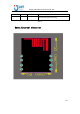
Jiangsu JWT Electronics Shares CO.,Ltd. Wireless game equipment Wireless label Telemetry Wireless access Security System Intelligent sports equipment Remote Control Wireless toys Five.Internal circuit block diagram Picture 5 Six.Description of pin function Pin number Name type functional description 1 GND GND GND 2 VCC PWR 3.
Jiangsu JWT Electronics Shares CO.,Ltd. 7 MISO DI 8 IRQ DI SPI data output pin Transmit and receive status flag Table 6 Seven.
Jiangsu JWT Electronics Shares CO.,Ltd. Eight.Application wiring diagram 3.3V System application circuit Picture 8-1 Nine.PCB-layout and installation considerations Module considerations: 1. No line under the antenna, keep the antenna part clear。 2. 3.3V power supply should be kept stable and clean, If the noise or interference of 3.3V power supply is relatively large, it is suggested that the RF module should be supplied after the RC or LC filtering. 3.
Jiangsu JWT Electronics Shares CO.,Ltd. the module to avoid welding short circuit。 d. The MCU is used to drive software, which can communicate with other modules。 Warning: after all equipment has been installed, switch on power。 Ten.Communication Interface SPI time-sequential format Picture 10-1 Notes: 1. SPI to drop along sampling data,rise along the change data;MCU under control SPI_MOSI be bound after SPI_CLK raise that to change the data。 2. SPI read write bit: write=0,read=1。 3.
Jiangsu JWT Electronics Shares CO.,Ltd. Name Min Typ. Max Description T1 250ns Interval between two SPI visits T2a,T2b 41.5ns Interval between SPI_CS and SPI_CLK T3 Note1 Address and data interval T4 Note1 High byte and low byte interval T5 Note2 Interval between two registers T6 83ns Clock cycle of SPI_CLK picture 10-2 Notes: 1. In the FIFO data in the access register 0x28, the chip needs 450ns to find the correct pointer address read by FIFO. 2.
Jiangsu JWT Electronics Shares CO.,Ltd.
Jiangsu JWT Electronics Shares CO.,Ltd.
Jiangsu JWT Electronics Shares CO.,Ltd. 11: reserve, same as 00 3 2-0 brclk_sel[2:0] R/W 000: brclk keep 0 001: xtal_core out 010: crystal divided by 6, 2M out 011: crystal divided by 12, 1M out 100: APLL_clk out 101: clk_tx_out 000 Table 11-4 Operating configuration Register 0x07 default: 0x7311 Bit Name R/W 15 EN_VCO_CAL_IDLE R/W 14 TXRX_VCO_CAL_EN R/W 1: In TX/RX state, automatically calibrated R/W VCO automatic calibration waiting time in TXRX state: 0000: 12us 0001: 14us .......
Jiangsu JWT Electronics Shares CO.,Ltd. Rx_ack_time[5:0] (More than this time, if you haven't received an ACK signal back, it will automatically resend) Table 11-6 Timing configuration Register 0x0c default: 0x3E11 Bit Name R/W Description Default After starting TX/RX state, wait for VCO to stabilize time: 15-10 9-8 7-4 3-0 VCO_ON_DLY[5:0] TX_PA_OFF_DLY[1: 0] TX_PA_ON_DLY[3: 0] TX_SW_ON_DELAY [3:0] 000000: 4us 000001: 8us .........
Jiangsu JWT Electronics Shares CO.,Ltd. 15-14 13 FIFO_FLAG R 12 reserved R VCO_CAL_ERROR R 1: FIFO An empty or full mark bit 11 10 1: VCO Calibration failure 9-0 Table 11-9 Main status Register 0x16 Read only Bit Name R Description 15 CRC_error R 1: CRC wrong 0: CRC correct 14 FEC23_error R 1 : FEC23 wrong 0: FEC23 correct Framer state: 31H: ST_SLEEP 33H: ST_WAKE_UP......... ..........
Jiangsu JWT Electronics Shares CO.,Ltd. 14-0 R/W Table 11-11 Operating Control Register 0x1e default: 0x7FF4 Bit Name R/W 15-14 R/W 7FF4H Description Default Optim 1:Open software reset function, 1 is valid. 0 Reg_Reset_EN R/W the reset of the chip can be accomplished by enabling the rewriteable regicao 7 to 1 to be 1 .
Jiangsu JWT Electronics Shares CO.,Ltd.
Jiangsu JWT Electronics Shares CO.,Ltd.
Jiangsu JWT Electronics Shares CO.,Ltd.
Jiangsu JWT Electronics Shares CO.,Ltd. 1.Chip internal integration (POR) (if only internal reset, RST N feet only need to be raised or suspended), T1 time for power reset time, about 0.5ms 2. T2 is the crystal oscillator stabilization time, about 10ms, and then the register is initialized by the MCU 3. After the register is initialized, the chip can start transmitting or receiving data 4.
Jiangsu JWT Electronics Shares CO.,Ltd. 2、Enter sleep mode and wake up When the SPI CS pulls high, and the MCU writes register 0x01 [15], the chip enters the sleep mode, and the current <1uA, the value of the register in the sleep mode can be maintained. When SPI CS is low, the chip automatically wakes up into IDLE state. The MCU will pull the SPI CS for a period (wait for crystal stability, about 1.5ms), and then write the SPI data. 3、Packet format Air packet format Preamble: 1~8 bytes,Can be set up.
Jiangsu JWT Electronics Shares CO.,Ltd. 5、clean FIFO hand The read-write pointer that receives FIFO and sends FIFO can be removed by writing '1' at 0x25, 0x26 corresponding register。When the packet is received, the read pointer indicates how much bytes data is in FIFO. When the receiver receives SYNC, the receiving FIFO writes the pointer automatically 0. When the emitter sends out the data, a FIFO reading pointer automatically clears 0.
Jiangsu JWT Electronics Shares CO.,Ltd. 7、The state machine determines the length of the package When register 0x01[2]= 1, the first byte of payload indicates the package length, and the maximum length is 64 bytes 1、Launch timing Below shows TX time series: when MCU writes register 0x00[15] to '1', and write register 0x00[6:0] to set up the transmitting channel, the chip will automatically generate the package according to the payload. MCU needs to write the launch data before launching the trailer.
Jiangsu JWT Electronics Shares CO.,Ltd. MCU sending data packet flow chart FIFO and PKT flags are used as interrupt signals of MCU In the above flow chart, you can send the state machine first, then send data to send FIFO, which can improve MCU efficiency, but ensure that all data is written before the packet is sent. If the time required to write is very long, you should write all the data before starting the sending state.
Jiangsu JWT Electronics Shares CO.,Ltd. 2、Receive sequence The RX reception sequence is shown below. When MCU writes register 0x00[14] to 1 and selects a good receiver channel, the chip will open RX and wait for the correct syncword. When the correct syncword is received, the chip will automatically start processing the packets. When the packet is processed, the state machine will enter IDLE. When received packets longer than 63 bytes, FIFO flag will work, meaning that the MCU must read data from FIFO.
Jiangsu JWT Electronics Shares CO.,Ltd.
Jiangsu JWT Electronics Shares CO.,Ltd. failure, resend twice. Write register 0x0b[5:0], setting time, waiting for an ACK default is 0 x3f, each step is 16 us, a total of approximately 1 ms, said if the received an ACK packet waiting time of 1 ms and retransmission times no will to send packets to the maximum.
Jiangsu JWT Electronics Shares CO.,Ltd. length is determined by the state of register 0x01 [1]. 1、fw_term_tx=1 When register 0 x01 [1] = 1, when the firing data, the system will send FIFO write pointer and read pointer, if the MCU to stop sending FIFO data written, chips will eventually detected when the FIFO is empty, and then automatically exit status.
Jiangsu JWT Electronics Shares CO.,Ltd. Picture 13-6 2、fw_term_tx=0(TX) When register 0x01[2:1]=2 'b00, the system only stops firing when the register 0x00[15] tx en=0.
Jiangsu JWT Electronics Shares CO.,Ltd. Picture 13-8 3、fw_term_tx=0 (RX) When Reg0x01[2]= 0, the chip will start receiving the package at Reg0x00[14] when it is written as 1 (RX EN= 1), and the chip will automatically set the RX to the fixed channel. After waiting for some time to stabilize the internal clock and the RX circuit, the chip began to look for syncword in the received signal, and once found, it would pull the PKT FLAG and write the received data to FIFO.
Jiangsu JWT Electronics Shares CO.,Ltd. Picture 13-10 4、 PA Output power setting . The output power of PA can be set by register reg0x02. The maximum output power can reach +8dBm, and the minimum can reach -24dBm. The following table lists some power configurations (if you need other power configurations, please contact the company’s technical staff) The change of the power supply voltage will cause the output power to also change, so you need to pay attention to it in practical application.
Jiangsu JWT Electronics Shares CO.,Ltd. 5、RSSI Support RSSI detection function, in RX state, can read real-time RSSI directly through reg0x11[15:8] (1)、Set the chip to the RX state; (2)、The reg0x1c[15] was first written as 1, and the RSSI was closed to eliminate the remaining RSSI values. Then, the reg0x1c[15] is then written as 0, and the RSSI detection function is opened. After waiting for 60us, the current RSSI value can be read through reg0x11 [15:8].
Jiangsu JWT Electronics Shares CO.,Ltd. Picture 13-11 Forteen、FAQ 1、How to troubleshoot the SPI/I2C interface a、First check whether the power supply of the chip is normal, whether the VDD33 foot has voltage (3.3 V) input, and the RF VDD foot has 1.8V or so voltage output; b、Check the vibration of the chip. The default is IDLE state after the power is reset on the chip, and the crystal is switched on, and the power consumption is about 0.6 mA.
Jiangsu JWT Electronics Shares CO.,Ltd. 2、There are several main types of chips There are four main types of chips: 1、 IDLE state:When the chip is on (reset) the default is IDLE state, when the crystal is switched on, and the power consumption is about 0.
Jiangsu JWT Electronics Shares CO.,Ltd. write reg[0x05] = 0x7fa6; write reg[0x0A] = 0x2053; write reg[0x0D] = 0x6003; write reg[0x0F] = 0x661d; write reg[0x1A] = 0x00f7; write reg[0x01] = 0x207f; write reg[0x0B] = 0x857f; b、Clear to send FIFO write reg[0x26] = 0x8080 c、Write data to FIFO, such as the data sent: 0x05 0x01 0x02 0x03 0x04 0x05(The first byte represents length, the last five bytes are data, and the total length is 6 bytes.
Jiangsu JWT Electronics Shares CO.,Ltd.
Jiangsu JWT Electronics Shares CO.,Ltd. 5、 PKT_FALG How does the state change After the TX is started, the PKT FLAG will automatically pull down, the PKT FLAG will be raised after the data is sent, and then the PKT FLAG will remain high until the TX or RX is started again.
Jiangsu JWT Electronics Shares CO.,Ltd. will be automatically entered into a state of receiving, waiting for the receiver returns an ACK signal, if in a certain period of time (the time by0x0b[5:0] set, the default value is 0 x3f, about 1 ms) did not receive an ACK signal, then again send it again until it receives an ACK signal data or resend to reach maximum. The above process is automatically completed within the chip, without the need MCU intervention.
Jiangsu JWT Electronics Shares CO.,Ltd. 9、How to prevent FIFO overflow In sending or receiving data packets, in order to prevent spillage, FIFO can be set up by reg0x24 register the corresponding threshold, more than the threshold, the chip will give instructions, the indicator can be reg0x12 [13] FLAG (FIFO) to read. 10 、 Instructions for improving the working reliability of the chip In order to improve the reliability of the chip and the product yield, the following improvements are recommended: 1.
Jiangsu JWT Electronics Shares CO.,Ltd. edebrouillage,et(2)l'utilisateurdel'appareildoitacceptertoutbrouillageradioélectriquesubi,mêmesil ebrouillageestsusceptibled'encompromettrelefonctionnement." FCC STATEMENT : This device complies with Part 15 of the FCC Rules. Operation is subject to the following two conditions: This device may not cause harmful interference, and This device must accept any interference received, including interference that may cause undesired operation.
requirement instructions for host product manufacturers according to KDB 996369 D03 OEM Manual v01 2.2List of applicable FCC rules FCC Part 15 Subpart C 15.249 & 15.207 & 15.209 2.3 Specific operational use conditions This device is intended only for OEM integrators under the following conditions: The module must be installed in the host equipment such that 20 cm is maintained between the antenna and users, and the transmitter module may not be co-located with any other transmitter or antenna.
2.6RF exposure considerations This equipment complies with FCC radiation exposure limits set forth for an uncontrolled environment. This equipment should be installed and operated with a minimum distance of 20cm between the radiator & your body. This transmitter must not be co-located or operating in conjunction with any other antenna or transmitter. 2.7Antennas Antenna Type: PCB Antenna Antenna Gain(Peak):1.96 dBi 2.