
Wiring Diagram

Jiangsu JWT Electronics Shares CO.,Ltd.
15 / 42
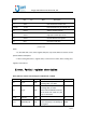
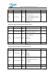
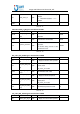
11: reserve, same as 00
3
2-0
brclk_sel[2:0]
R/W
000: brclk keep 0
001: xtal_core out
010: crystal divided by 6, 2M out
011: crystal divided by 12, 1M out
100: APLL_clk out
101: clk_tx_out
000
Table 11-4
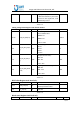
Operating configuration Register 0x07 default: 0x7311
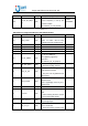
Bit
Name
R/W
Description
Default
15
EN_VCO_CAL_IDLE
R/W
1:Manually enable the VCO
calibration process in IDLE state
0
14
TXRX_VCO_CAL_EN
R/W
1: In TX/RX state, VCO is
automatically calibrated
1
13-10
TXRX_vco_tim[3:0]
R/W
VCO automatic calibration waiting
time in TXRX state:
0000: 12us
0001: 14us
.......
1111: 42us
1100
9-0
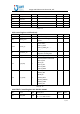
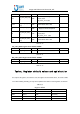
Table 11-5
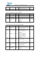
Timing configuration Register 0x0b default: 0x837F
Bit
Name
R/W
Description
Default
15-12
TX_CW_DLY[3:0]
R/W
PA After opening, send the CW's
time:
0000: 4us
0001: 6us
1111: 34us
1000
11-8
Re_transmit_time
R/W
ACK When the function is turned on,
the maximum retransmission:
2H: 2 times
3H: 3 times
.......
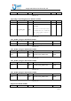
0011
7-6
R/W
01
5-0
Rx_ack_time[5:0]
R/W
The time the transmitter waits for
ACK to return : T=16us x
111111