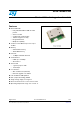
SPBT2632C2A Bluetooth® technology class-2 module Datasheet − production data Features ■ Bluetooth® radio – Fully embedded Bluetooth® v3.0 with profiles – Class 2 module – Complete RF ready module – 128-bit encryption security – Integrated antenna – Multipoint capability ■ ST micro Cortex-M3 microprocessor up to 72 MHz ■ Memory – 256 kb Flash memory – 48 kb RAM memory ■ Data rate – 1.5 Mbps maximum data rate ■ Serial interface – UART up to 2.
Contents SPBT2632C2A Contents 1 Description . . . . . . . . . . . . . . . . . . . . . . . . . . . . . . . . . . . . . . . . . . . . . . . . . 6 2 RoHS compliance . . . . . . . . . . . . . . . . . . . . . . . . . . . . . . . . . . . . . . . . . . . 7 3 Applications . . . . . . . . . . . . . . . . . . . . . . . . . . . . . . . . . . . . . . . . . . . . . . . . 7 4 Software architecture . . . . . . . . . . . . . . . . . . . . . . . . . . . . . . . . . . . . . . . . 8 5 4.1 Lower layer stack . . . .
SPBT2632C2A Contents 7.6 External LPO input circuit . . . . . . . . . . . . . . . . . . . . . . . . . . . . . . . . . . . . . 20 7.7 Apple iOS CP reference design . . . . . . . . . . . . . . . . . . . . . . . . . . . . . . . . 21 8 Regulatory compliance . . . . . . . . . . . . . . . . . . . . . . . . . . . . . . . . . . . . . . 23 9 Ordering information . . . . . . . . . . . . . . . . . . . . . . . . . . . . . . . . . . . . . . . 25 10 Revision history . . . . . . . . . . . . . . . . . . . . . .
List of tables SPBT2632C2A List of tables Table 1. Table 2. Table 3. Table 4. Table 5. Table 6. Table 7. Table 8. Table 9. Table 10. Table 11. 4/27 Recommended operating conditions . . . . . . . . . . . . . . . . . . . . . . . . . . . . . . . . . . . . . . . . . 10 Absolute maximum ratings . . . . . . . . . . . . . . . . . . . . . . . . . . . . . . . . . . . . . . . . . . . . . . . . . 10 High speed CPU mode current consumption . . . . . . . . . . . . . . . . . . . . . . . . . . . . . . . . . . .
SPBT2632C2A List of figures List of figures Figure 1. Figure 2. Figure 3. Figure 4. Figure 5. Figure 6. Figure 7. Figure 8. Figure 9. Figure 10. Figure 11. Figure 12. Figure 13. Figure 14. FW architecture . . . . . . . . . . . . . . . . . . . . . . . . . . . . . . . . . . . . . . . . . . . . . . . . . . . . . . . . . . 9 Pin placement . . . . . . . . . . . . . . . . . . . . . . . . . . . . . . . . . . . . . . . . . . . . . . . . . . . . . . . . . . . 14 Layout drawing . . . . . . . . . . . . . . . . . .
Description 1 SPBT2632C2A Description The SPBT2632C2A.AT2 is an easy to use Bluetooth module, compliant with Bluetooth v3.0. The module is the smallest form factor available which provides a complete RF platform. The SPBT2632C2A.AT2 enables electronic devices with wireless connectivity, not requiring any RF experience or expertise for integration into the final product. The SPBT2632C2A.AT2 module, being a certified solution, optimizes the time to market of the final applications.
SPBT2632C2A 2 RoHS compliance RoHS compliance ST modules are RoHS compliant and comply with ECOPACK® norms. 3 Applications ● Serial cable replacement ● M2M industrial control ● Service diagnostic ● Data acquisition equipment ● Machine control ● Sensor monitoring ● Security system ● Mobile health.
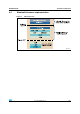
Software architecture SPBT2632C2A 4 Software architecture 4.1 Lower layer stack 4.2 4.3 ● Bluetooth v3.
SPBT2632C2A 4.4 Software architecture Bluetooth firmware implementation Figure 1.
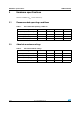
Hardware specifications 5 SPBT2632C2A Hardware specifications General conditions (VIN = 2.5 V and 25 °C). 5.1 Recommended operating conditions Table 1. 5.2 Rating Min. Typical Max. Unit Operating temperature range -40 - 85 °C Supply voltage VIN 2.1 2.5 3.6 V Signal pin voltage - 2.1 - V RF frequency 2400 - 2483.5 MHz Absolute maximum ratings Table 2. 10/27 Recommended operating conditions Absolute maximum ratings Rating Min. Typical Max.
SPBT2632C2A 5.3 Hardware specifications High speed CPU mode current consumption ● High speed CPU mode – CPU 32 MHz – UART supports up to 921 Kbps – Data throughput up to 1.5 Mbps – Shallow sleep enabled. Table 3. High speed CPU mode current consumption Modes (typical power consumption) 5.4 Avg. Unit ACL data 115 K baud UART at max. throughput (master) 23 mA ACL data 115 K baud UART at max. throughput (slave) 27.5 mA Connection, no data traffic, master 9.
Hardware specifications Table 4. SPBT2632C2A Standard CPU mode current consumption (continued) Modes (typical power consumption) 5.5 Unit Standby, with deep sleep, with external LPO 70 µA Page/inquiry scan, with deep sleep, no external LPO 2.6 mA Page/inquiry scan, with deep sleep, with external LPO 520 µA Bluetooth power-down / CPU standby, no external LPO 25 µA I/O operating characteristics Table 5. 5.6 Avg. I/O operating characteristics Symbol Parameter Min. Max.
SPBT2632C2A 5.7 Hardware specifications Pin assignment Table 7. Name Pin assignment Type Pin# Description ALT function(1) 5V tolerant ADC 3 Y ADC 2 Y UART interface RXD I 13 Receive data TXD O 14 Transmit data 2 RTS O 12 Request to send (active low) ADC 0 I C clock/aux UART Rx Y CTS I 11 Clear to send (active low) ADC 1 I2C data/aux UART Tx Y Boot loader Boot 0 I 9 Boot 0 Power and ground Vin 8 Vin GND 7 GND Reset RESETN I 10 2.5 V max.
Hardware specifications 5.8 SPBT2632C2A Pin placement Figure 2. Pin placement !- V 5.9 Layout drawing Figure 3.
SPBT2632C2A 6 Hardware block diagram Hardware block diagram Figure 4. SPBT2632C2A.AT2 module block diagram %DWWHU\ RU 6XSSO\ $50 &RUWH[ 0&8 670 5HJXODWRU $QWHQQD . )ODVK %3 )LOWHU +RVW &RQWUROOHU ,QWHUIDFH 67/& 8$57 *3,2 .
Hardware design 7 SPBT2632C2A Hardware design The SPBT2632C2A module without AT2 command embedded FW supports UART, SPI, I2C and GPIO hardware interfaces. Note that the usage of these interfaces is dependent upon the firmware that is loaded into the module, and is beyond the scope of this document. The AT2 command interface uses the main UART by default. Note: 7.1 1 All unused pins should be left floating; do not ground. 2 All GND pins must be well grounded.
SPBT2632C2A Hardware design Figure 5. Soldering profile !- V 7.2 GPIO interface All GPIOs are capable of sinking and sourcing 4 mA of I/O current. GPIO [1] to GPIO [7] are internally pulled down with 100 kΩ (nominal) resistors. 7.3 UART interface The UART is compatible with the 16550 industry standard. Four signals are provided with the UART interface. The TXD and RXD pins are used for data while the CTS and RTS pins are used for flow control. Figure 6.
Hardware design Figure 7. SPBT2632C2A Typical RS232 circuit !- V 7.4 PCB layout guidelines Figure 8.
SPBT2632C2A 7.5 Hardware design Reset circuit Two types of system reset circuits are detailed below. 7.5.1 External reset circuit Figure 9. External reset circuit 2%3%4 !- V Note: RPU ranges from 30 kΩ to 50 kΩ internally. 7.5.2 Internal reset circuit Figure 10. Internal reset circuit 2%3%4 !- V Note: 1 RPU ranges from 30 kΩ to 50 kΩ internally. 2 RRST should be from 1 kΩ to 10 kΩ.
Hardware design 7.6 SPBT2632C2A External LPO input circuit An optional low power oscillator input may be added to allow Deep sleep and Sniff modes. ● ● LPO parameters: – Frequency: 32.768 kHz – Tolerance: 150 ppm – Voltage levels – Low: 0.5 V – High: 1.8 V – Input capacitance: 2.5 pF maximum Configurations: – Table 9. Use two configuration variables: UseExtLPO and AllowSniff. System configuration variables Variable Name Default Description Var37 UseExtLPO True True when a 32.
SPBT2632C2A 7.7 Hardware design Apple iOS CP reference design The figures below give an indicative overview of what the hardware concept looks like. A specific MFI co-processor layout is available for licensed MFI developers from the MFI program. Figure 12. BT module !- V Figure 13.
Hardware design SPBT2632C2A Figure 14.
SPBT2632C2A 8 Regulatory compliance Regulatory compliance ● FCC and IC – This module has been tested and found to comply with the FCC part 15 and IC RSS-210 rules. These limits are designed to provide reasonable protection against harmful interference in approved installations. This equipment generates, uses, and can radiate radio frequency energy and, if not installed and used in accordance with the instructions, may cause harmful interference to radio communications.
Regulatory compliance ● SPBT2632C2A CE – CE Expert opinion: 0448-ARAM00003 – Measurements have been performed in accordance with (report available on request): – EN 300 328 V 1.7.1 (2006-10) (a) – EN 301 489-17 V 2.1.1 (2009) (b) – EN60950-1:2006 +A11:2009+A1:2010 (c) CE certified: a. EN 300 328 V 1.7.1 (2006-10): “electromagnetic compatibility and radio spectrum Matters (ERM); Wideband transmission systems; data transmission equipment operating in the 2.
SPBT2632C2A 9 Ordering information Ordering information Table 10. Ordering information Order code Description SPBT2632C2A.
Revision history 10 SPBT2632C2A Revision history Table 11. 26/27 Document revision history Date Revision Changes 03-Apr-2012 1 First release.
SPBT2632C2A Please Read Carefully: Information in this document is provided solely in connection with ST products. STMicroelectronics NV and its subsidiaries (“ST”) reserve the right to make changes, corrections, modifications or improvements, to this document, and the products and services described herein at any time, without notice. All ST products are sold pursuant to ST’s terms and conditions of sale.