a module solution provider WG6031-00 WLAN Module Realtek RTL8189EM IEEE 802.11b/g/n 1T/1R Solution with SDIO/SPI Interface Datasheet Draft 0.2 Prepared By Reviewed By Copyright © JORJIN TECHNOLOGIES INC. 2017 http://WWW.JORJIN.COM.
Doc No: WG6031-00-DTS-D02 Index 1. HISTORY CHANGE .............................................................................................................................. 2 2. GENERAL DESCRIPTION ..................................................................................................................... 3 2.1. FEATURES........................................................................................................................................ 3 3. MODULE BLOCK DIAGRAM .............
Doc No: WG6031-00-DTS-D02 1. HISTORY CHANGE Revision Date Description Draft 0.1 2017-06-05 Initial Document creation. Draft 0.2 2017-10-06 1. 2. 3. 4. Updated SDIO information. Corrected RF Performance. Updated Module Size tolerance. Added Module Package Marking and Regulatory Information. Copyright © JORJIN TECHNOLOGIES INC. 2017 http://WWW.JORJIN.COM.
Doc No: WG6031-00-DTS-D02 2. GENERAL DESCRIPTION The WG6031-00 is a 802.11b/g/n 1T1R Wireless LAN SiP (system in package) module with SDIO/SPI interface. The WG6031-00 provides a complete solution for a high throughput performance integrated wireless LAN device. 2.1. Features Dimension 13mm(L) x 13mm(W) x 2.35mm(H). LGA-20 pin package. CMOS MAC, Baseband PHY, and RF in a single chip for 802.11b/g/n compatible WLAN. Complete 802.11n solution for 2.4GHz band. 72.2Mbps receive PHY rate and 72.
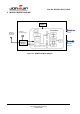
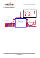
Doc No: WG6031-00-DTS-D02 3. MODULE BLOCK DIAGRAM Xtal 40MHz External RF Design (Default) Internal RF Connector RTL8189EM VDD33 TX/RX Matching Circuit SDIO/SPI Interface Figure 3-1. WG6031-00 Block Diagram Copyright © JORJIN TECHNOLOGIES INC. 2017 http://WWW.JORJIN.COM.
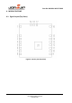
Doc No: WG6031-00-DTS-D02 4. MODULE OUTLINE 4.1. Signal Layout (Top View) Figure 4-1 Device pins (Top View) Copyright © JORJIN TECHNOLOGIES INC. 2017 http://WWW.JORJIN.COM.
Doc No: WG6031-00-DTS-D02 4.2.
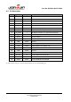
Doc No: WG6031-00-DTS-D02 5. MODULE SPECIFICATION 5.1. General Module Requirements and Operation 5.1.1. Temperature Limit Ratings Parameter Min Max Units Storage Temperature -40 +125 ℃ Ambient Operating 0 +70 ℃ 5.1.2. DC Power Supply Characteristics Parameter Condition Min Typical Max Units VDD DC supply Voltage 3.0 3.3 3.6 V 5.1.3. Digital IO DC Characteristics Parameter Condition Min Normal Max Units VIH Input high voltage 2.0 3.3 3.6 V VIL Input low voltage - 0 0.
Doc No: WG6031-00-DTS-D02 5.2. WLAN RF Performance 5.2.1. WLAN 2.4-GHz Receiver Characteristics Parameter Condition Min Operation frequency range 2412 At < 8% PER limit Sensitivity Typ At < 10% PER At < 10% PER limit 1 Mbps DSSS -95 11 Mbps CCK -86 6 Mbps OFDM -91 54 Mbps OFDM -74 MCS0 MM -90 MCS7 MM -71 MCS0 MM 40MHz -87 MCS7 MM 40MHz -68 Max Units 2484 MHz dBm 5.2.2. WLAN 2.
Doc No: WG6031-00-DTS-D02 6. REFERENCE SCHEMATICS C8 10pF CAP1005 1 ANT1 2 RF_OUT L1 NL IND1005 L2 NL IND1005 PIN-4 defined as SDIO_D3 if SDIO interface. 2 3 1 TP1 C3 C4 C5 C6 NU 0402 NU 0402 NU 0402 NU 0402 SPI_IRQ R1 SPI_SS R2 SPI_MISO R3 SPI_MOSI R5 4 5 0R 0402 6 0R 0402 7 0R 0402 8 0R 0402 17 GND 19 18 RF OUT GND PGND 1 GND 20 Pi-Circuit for Antenna matching. GND GND U1 GND GND WG6031-00 Module 3.3V NC/SD_D3 E-13X13-N20-1.2-TOP 3.
Doc No: WG6031-00-DTS-D02 7. PACKAGE INFORMATION 7.1. Module mechanical outline Figure 6-1 Module Pad Dimensions Copyright © JORJIN TECHNOLOGIES INC. 2017 http://WWW.JORJIN.COM.
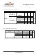
Doc No: WG6031-00-DTS-D02 Marking L (Body size) W (Body size) T (Thickness) a a1 a2 a3 Min 12.85 12.85 2.15 0.55 1.05 1.15 3.55 Nom 13.00 13.00 2.35 0.60 1.10 1.20 3.60 Max 13.15 13.15 2.55 0.65 1.15 1.25 3.65 Marking b b1 b2 b3 c c1 c2 Min 0.75 0.10 4.65 5.85 2.95 7.55 4.45 Nom 0.80 0.15 4.70 5.90 3.00 7.60 4.50 Max 0.85 0.20 4.75 5.95 3.05 7.65 4.55 Table 7-1. Dimensions for Module Mechanical Outline 7.2. Ordering Information Part number: WG6031-00A 7.3.
Doc No: WG6031-00-DTS-D02 8. SMT AND BAKING RECOMMENDATION 8.1. Baking Recommendation Baking condition: - Follow MSL Level 4 to do baking process. After bag is opened, devices that will be subjected to reflow solder or other high temperature process must be a) Mounted within 72 hours of factory conditions <30°C/60% RH, or b) Stored at <10% RH. - Devices require bake, before mounting, if Humidity Indicator Card reads >10% If baking is required, Devices may be baked for 8 hrs at 125 °C. 8.2.
Doc No: WG6031-00-DTS-D02 No. Item Temperature (°C) Time (sec) 1 Pre-heat D1: 140 ~ D2: 200 T1: 80 ~ 120 2 Soldering D2: = 220 T2: 60 ± 10 3 Peak-Temp. D3: 250 °C max Note: (1) Reflow soldering is recommended two times maximum. (1) Add Nitrogen while Reflow process: SMT solder ability will be better. Stencil thickness: 0.1~ 0.15 mm (Recommended) Soldering paste (without Pb): Recommended SENJU N705-GRN3360-K2-V can get better soldering effects. Copyright © JORJIN TECHNOLOGIES INC.
Doc No: WG6031-00-DTS-D02 9. REGULATORY INFORMATION This section outlines the regulatory information for the following countries: United States Europe Japan 9.1. United States Federal Communications Commission Statement This equipment has been tested and found to comply with the limits for a Class B digital device, pursuant to Part 15 of the FCC Rules. These limits are designed to provide reasonable protection against harmful interference in a residential installation.
Doc No: WG6031-00-DTS-D02 FCC RF Radiation Exposure Statement: This device complies with FCC radiation exposure limits set forth for an uncontrolled environment and it also complies with Part 15 of the FCC RF Rules.