a module solution provider ZB7412-00 SimpleLinkTM Bluetooth® Low Energy Wireless MCU Module TI CC2640R2F Solution Datasheet Revision 0.3 Prepared By Reviewed By Approved By ----------------------------------------------------------------------------------------------------------------------------- --------------------Copyright © JORJIN TECHNOLOGIES INC. 2017 http://WWW.JORJIN.COM.
DOC No: ZB7412-00A-DTS-R03 Index 1. OVERVIEW ....................................................................................................................................... 3 1.1. GENERAL FEATURES ........................................................................................................................ 3 1.2. APPLICATIONS ................................................................................................................................ 4 2. FUNCTIONAL FEATURES ...........
DOC No: ZB7412-00A-DTS-R03 4.20. BATTERY MONITOR ..................................................................................................................... 24 4.21. CONTINUOUS TIME COMPARATOR ................................................................................................. 24 4.22. LOW-POWER CLOCKED COMPARATOR............................................................................................. 24 4.23. PROGRAMMABLE CURRENT SOURCE ...........................................
DOC No: ZB7412-00A-DTS-R03 1. OVERVIEW The certified ZB7412-00 module from JORJIN is a wireless MCU module targeting Bluetooth 4.2 and Bluetooth 5 low energy applications. This module is based on TI CC2640R2F wireless MCU QFN-32 package chip. The module is a cost-effective, ultralow power, 2.4-GHz RF devices. Very low active RF and MCU current and low-power mode current consumption provide excellent battery lifetime and allow for operation on small coin cell batteries and in energy-harvesting applications.
DOC No: ZB7412-00A-DTS-R03 - Code Composer Studio™ 1.2.
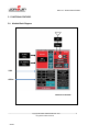
DOC No: ZB7412-00A-DTS-R03 2. FUNCTIONAL FEATURES 2.1. Module Block Diagram VDD GPIOs ZB7412-00 module ____________________________________________________________________________________ Copyright © JORJIN TECHNOLOGIES INC. 2017 5 http://WWW.JORJIN.COM.
DOC No: ZB7412-00A-DTS-R03 2.2.
DOC No: ZB7412-00A-DTS-R03 AES-128 Security Module True Random Number Generator (TRNG) Support for 8 Capacitive Sensing Buttons Integrated Temperature Sensor RF Section 2.4 GHz RF Transceiver Compatible With Bluetooth Low Energy (BLE) 4.2 and 5 specifications Excellent Receiver Sensitivity (–96 dBm for BLE), Selectivity, and Blocking Performance Link budget of 101 dB for BLE.
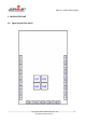
DOC No: ZB7412-00A-DTS-R03 3. MODULE OUTLINE 3.1. Signal Layout (Top View) ____________________________________________________________________________________ Copyright © JORJIN TECHNOLOGIES INC. 2017 8 http://WWW.JORJIN.COM.
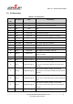
DOC No: ZB7412-00A-DTS-R03 3.2. Pin Description Table 3-1. Pin Description Pin No.
DOC No: ZB7412-00A-DTS-R03 21 DIO_14 Digital/Analog I/O 22 VDDS Power 1.8 V to 3.8 V main chip and DC/DC supply 23 VDDS2 Power 1.8 V to 3.8 V GPIO supply 24 NC 25 GND GND Ground G1~G4 GND GND Ground NC GPIO, Sensor Controller, Analog No connection. ____________________________________________________________________________________ Copyright © JORJIN TECHNOLOGIES INC. 2017 10 http://WWW.JORJIN.COM.
DOC No: ZB7412-00A-DTS-R03 4. MODULE SPECIFICATIONS 4.1. Absolute Maximum Ratings(1)(2) over operating free-air temperature range (unless otherwise noted) Parameter Supply voltage, VDDS Conditions (3) Voltage on any digital pin (4) MIN MAX Unit -0.3 4.1 V -0.3 VDDS+0.3 V Max 4.1 Voltage on ADC input (Vin) Voltage scaling enabled -0.3 VDDS V Internal reference, voltage scaling disabled -0.3 1.49 V VDDS as reference, voltage scaling disabled -0.3 VDDS/2.
DOC No: ZB7412-00A-DTS-R03 4.3. Recommended Operating Conditions Parameter Conditions Ambient temperature range Operating supply voltage (VDDS) For operation in battery-powered and MIN MAX Unit -40 85 °C 1.8 3.8 V 3.3 V systems ____________________________________________________________________________________ Copyright © JORJIN TECHNOLOGIES INC. 2017 12 http://WWW.JORJIN.COM.
DOC No: ZB7412-00A-DTS-R03 4.4. Power Consumption Summary Tc = 25°C, VDDS = 3.0 V with internal DC-DC converter, unless otherwise noted. Test Conditions Parameter Reset. RESET_N pin asserted or VDDS below Min Typ Max Units 100 nA Shutdown. No clocks running, no retention 150 nA Standby. With RTC, CPU, RAM and (partial) 1.1 μA 1.3 μA 2.8 μA 3.0 μA 550 μA Power-on-Reset threshold register retention. RCOSC_LF Standby. With RTC, CPU, RAM and (partial) register retention.
DOC No: ZB7412-00A-DTS-R03 4.5. General Characteristics Tc = 25°C, VDDS = 3.0 V, unless otherwise noted. Test Conditions Parameter Min Typ Max Units FLASH MEMORY Supported flash erase cycles 100 K before failure Cycles Flash page/sector erase current Flash page/sector erase time Average delta current (1) Flash page/sector size Flash write current Flash write time Average delta current, 4 bytes at a time (1) 4 bytes at a time Flash page/sector erase time (1) 12.6 mA 8 ms 4 KB 8.
DOC No: ZB7412-00A-DTS-R03 Selectivity, ±4 MHz (1) Wanted signal at –79 dBm, modulated interferer at ±4 MHz, BER = 10 Selectivity, ±6 MHz (1) Alternate channel rejection, ±7 MHz ≥ ±7 MHz, BER = 10 Selectivity, Image frequency 49/46 (2) dB 50/47 (2) dB –3 Wanted signal at -79 dBm, modulated interferer at (1) dB –3 Wanted signal at –79 dBm, modulated interferer at (1) (2) –3 Wanted signal at –79 dBm, modulated interferer at ±6 MHz, BER = 10 46/47 32 dB –3 image frequency, BER = 10
DOC No: ZB7412-00A-DTS-R03 300 440 Class 2 (Europe), FCC CFR47 Part 15 (US), and ARIB STD-T66 (Japan). 4.8. 500-kbps Coded (Bluetooth 5) – RX RF performance is specified in a single ended 50 ohm reference plane at the antenna feeding point with Tc = 25°C, VDDS = 3.0 V, fRF = 2440 MHz, unless otherwise noted.
DOC No: ZB7412-00A-DTS-R03 (1) ±8 MHz and above, BER = 10 MHz and above Out-of-band blocking (3) –3 30 MHz to 2000 MHz --35 dBm Out-of-band blocking 2003 MHz to 2399 MHz -19 dBm Out-of-band blocking 2484 MHz to 2997 MHz -19 dBm Intermodulation Wanted signal at 2402 MHz, -69 dBm.
DOC No: ZB7412-00A-DTS-R03 Co-channel rejection (1) Wanted signal at –67 dBm, modulated interferer in channel, BER = 10 Selectivity, ±1 MHz (1) Wanted signal at –67 dBm, modulated interferer at (1) dB 7/3 (2) dB –3 ±1 MHz, BER = 10 Selectivity, ±2 MHz -6 –3 Wanted signal at –67 dBm, modulated interferer at 34/25 (2) dB 38/26 (2) dB 42/29 (2) dB –3 ±2 MHz, BER = 10 Selectivity, ±3 MHz (1) Wanted signal at –67 dBm, modulated interferer at ±3 MHz, BER = 10 Selectivity, ±4 MHz (1)
DOC No: ZB7412-00A-DTS-R03 4.11. 1-Mbps GFSK (Bluetooth Low Energy) – TX RF performance is specified in a single ended 50 ohm reference plane at the antenna feeding point with Tc = 25°C, VDDS = 3.0 V, fRF = 2440 MHz, unless otherwise noted. Test Conditions Parameter Min Typ Max Units 3.2 4.8 5.
DOC No: ZB7412-00A-DTS-R03 frequency (1) –3 image frequency, BER = 10 Selectivity, Image 3/26(2) dB 30 MHz to 2000 MHz -33 dBm Out-of-band blocking 2003 MHz to 2399 MHz 15 dBm Out-of-band blocking 2484 MHz to 2997 MHz -12 dBm Out-of-band blocking 3000 MHz to 12.75 GHz -10 dBm Intermodulation Wanted signal at 2402 MHz, –64 dBm. Two -34 dBm frequency ±2 MHz Note that Image frequency +2 MHz is the (1) Co-channel.
DOC No: ZB7412-00A-DTS-R03 Crystal frequency tolerance Start-up time (2) -40 +40 (3) 150 ppm μs (1) Probing or otherwise stopping the XTAL while the DC-DC converter is enabled may cause permanent damage to the device. (2) Includes initial tolerance of the crystal, drift over temperature, aging and frequency pulling due to incorrect load capacitance. As per Bluetooth specification (3) Kick-started based on a temperature and aging compensated RCOSC_HF using precharge injection 4.15. 32.
DOC No: ZB7412-00A-DTS-R03 4.18. ADC Characteristics(1) Tc = 25°C, VDDS = 3.0 V and voltage scaling enabled, unless otherwise noted. Parameter Test Conditions Min Input voltage range Typ 0 Resolution Gain error Units VDDS V 12 Sample rate Offset Max Bits 200 ksps Internal 4.3-V equivalent reference (2) 2 LSB Internal 4.3-V equivalent reference (2) 2.4 LSB >-1 LSB ±3 LSB 9.8 Bits 10 Bits 11.
DOC No: ZB7412-00A-DTS-R03 Current consumption VDDS as reference 0.75 mA Reference voltage Equivalent fixed internal reference (input voltage 4.3 V scaling enabled). For best accuracy, the ADC (2)(4) conversion should be initiated through the TI-RTOS™ API to include the gain or offset compensation factors stored in FCFG1. Reference voltage Fixed internal reference (input voltage scaling 1.48 V VDDS V VDDS/ V disabled).
DOC No: ZB7412-00A-DTS-R03 4.20. Battery Monitor Tc = 25°C, VDDS = 3.0 V, unless otherwise noted. Test Conditions Parameter Min Typ Resolution Max 50 Range Units mV 1.8 3.8 Accuracy V mV 13 4.21. Continuous Time Comparator Tc = 25°C, VDDS = 3.0 V, unless otherwise noted. Test Conditions Parameter Min Typ Max Units Input voltage range 0 VDDS V External reference voltage 0 VDDS V Internal reference voltage DCOUPL as reference 1.27 V Offset 3 mV Hysteresis <2 mV 0.
DOC No: ZB7412-00A-DTS-R03 Hysteresis <5 Decision time Step from –50 mV to +50 mV Current consumption when enabled mV <1 clock cycle nA 362 4.23. Programmable Current Source Tc = 25°C, VDDS = 3.0 V, unless otherwise noted. Test Conditions Parameter Min Current source programmable output range Resolution Current consumption (1) Including current source at Typ Max Units 0.25-20 μA 0.
DOC No: ZB7412-00A-DTS-R03 TA = 25°C, VDDS = 3.8 V GPIO pullup current Input mode, pullup enabled, Vpad = 0 V 277 μA GPIO pulldown current Input mode, pulldown enabled, Vpad = VDDS 113 μA GPIO high/low input IH = 0, transition between reading 0 and reading 1 1.67 V IH = 1, transition voltage for input read as 0→1 1.94 V IH = 1, transition voltage for input read as 1→0 1.54 V IH = 1, difference between 0→1 and 1→0 points 0.
DOC No: ZB7412-00A-DTS-R03 4.22. (5) Refer to SSI timing diagrams Figure 4-1, Figure 4-2, and Figure 4-3. 4.26. Switching Characteristics Tc = 25°C, VDDS = 3.0 V, unless otherwise noted.
DOC No: ZB7412-00A-DTS-R03 Figure 4-2. SSI Timing for MICROWIRE Frame Format (FRF = 10), Single Transfer Figure 4-3. SSI Timing for SPI Frame Format (FRF = 00), With SPH = 1 ____________________________________________________________________________________ Copyright © JORJIN TECHNOLOGIES INC. 2017 28 http://WWW.JORJIN.COM.
DOC No: ZB7412-00A-DTS-R03 4.27. Typical Characteristics There are some typical performance plots measured on the CC2640R2FRHB device in the CC2640R2F data sheet, and the plots relevant for the ZB7412-00 module. Please visit TI web site http://www.ti.com/lit/gpn/cc2640r2f , and see Section 5.29 ____________________________________________________________________________________ Copyright © JORJIN TECHNOLOGIES INC. 2017 29 http://WWW.JORJIN.COM.
DOC No: ZB7412-00A-DTS-R03 4.28. Chip Antenna Characteristics Measured on the Jorjin ZB7412E00 EM board with TA = 25°C Parameter 2400MHz 2442MHz 2484MHz Efficiency% 57.6 % 59.1 % 58.9 % Peak Gain 2.0 dBi 2.2 dBi 2.3 dBi Figure 4-4. Efficiency vs. Frequency Z ____________________________________________________________________________________ Copyright © JORJIN TECHNOLOGIES INC. 2017 30 http://WWW.JORJIN.COM.
DOC No: ZB7412-00A-DTS-R03 Z Y X Z Y Figure 4-5. DUT 3D Pattern ____________________________________________________________________________________ Copyright © JORJIN TECHNOLOGIES INC. 2017 31 http://WWW.JORJIN.COM.
DOC No: ZB7412-00A-DTS-R03 5. DESIGN RECOMMENDATIONS 5.1. Module Layout Recommendations Follow these module layout recommendations: Antenna For a module with on board chip antenna, to eliminate the influence from other components or ground, recommended that the module is placed in the corner of main PCB, and define a clearance area around the antenna, where no grounding or signal trace are contained. The clearance area applies to all layers of the main PCB.
DOC No: ZB7412-00A-DTS-R03 RF test point There are RF test points in the bottom side of this module. It is only for module production used. Do not connect any signal to these test points (leave no connection) in the module. And do not design test point in the main board. Please reserve a clearance in the top-side copper plane underneath the RF test pads. Do not route any signal or place via in this keep out area.
DOC No: ZB7412-00A-DTS-R03 5.2.
DOC No: ZB7412-00A-DTS-R03 6. PACKAGE INFORMATION 6.1. Module Mechanical Outline Top View Note: 1> Pad tolerance as ±30um 2> Unit: mm ____________________________________________________________________________________ Copyright © JORJIN TECHNOLOGIES INC. 2017 35 http://WWW.JORJIN.COM.
DOC No: ZB7412-00A-DTS-R03 Top and Side View Shielding case Opening Note: A: Typical: 2.45mm, Maximum: 2.69mm B: Typical: 2.00mm, Maximum: 2.20mm Unit: mm 6.2. Ordering Information Order Number Package ZB7412-00 LGA-25 ____________________________________________________________________________________ Copyright © JORJIN TECHNOLOGIES INC. 2017 36 http://WWW.JORJIN.COM.
DOC No: ZB7412-00A-DTS-R03 6.3.
DOC No: ZB7412-00A-DTS-R03 TELEC compliance mark, and ID CE compliance mark NCC compliance mark, and ID ____________________________________________________________________________________ Copyright © JORJIN TECHNOLOGIES INC. 2017 38 http://WWW.JORJIN.COM.
DOC No: ZB7412-00A-DTS-R03 7. SMT AND BAKING RECOMMENDATION 7.1. Baking Recommendation Baking condition: - Follow MSL Level 4 to do baking process. - After bag is opened, devices that will be subjected to reflow solder or other high temperature process must be a) Mounted within 72 hours of factory conditions <30°C/60% RH, or b) Stored at <10% RH. - Devices require bake, before mounting, if Humidity Indicator Card reads >10% - If baking is required, Devices may be baked for 8 hrs. at 125 °C. 7.2.
DOC No: ZB7412-00A-DTS-R03 No. Item Temperature (°C) Time (sec) 1 Pre-heat D1: 140 ~ D2: 200 T1: 80 ~ 120 2 Soldering D2: = 220 T2: 60 +/- 10 3 Peak-Temp. D3: 250 °C max Note: (1) Reflow soldering is recommended two times maximum. (2) Add Nitrogen while Reflow process: SMT solder ability will be better. Stencil thickness: 0.1~ 0.13 mm (Recommended) Soldering paste (without Pb): Recommended SENJU N705-GRN3360-K2-V can get better soldering effects.
DOC No: ZB7412-00A-DTS-R03 8. TAPE REEL INFROMATION 8.1. Cover / Carrier Tape Dimension Packing Qty Dry Bag Inner Box Outer Box 1200 EA / Reel 1 Reel (1200 EA) 1 Dry Bag (1200 EA) 4 Inner Box (4800 EA) Inner Box Size : 352mm x 352mm x 56mm Outer Box Size : 354mm x 362mm x 250mm ____________________________________________________________________________________ Copyright © JORJIN TECHNOLOGIES INC. 2017 41 http://WWW.JORJIN.COM.
DOC No: ZB7412-00A-DTS-R03 9. REGULATORY INFORMATION This section outlines the regulatory information for the following countries: United States Canada Europe Japan Taiwan Australia/New Zealand 9.1. United States Federal Communications Commission Statement 15.21. You are cautioned that changes or modifications not expressly approved by the part responsible for compliance could void the user’s authority to operate the equipment. This device complies with Part 15 of the FCC Rules.
DOC No: ZB7412-00A-DTS-R03 module. The end user manual shall include all required regulatory information/warning as shown in this manual. 9.2. Canada This device complies with Industry Canada’s licence-exempt RSS standard(s). Operation is subject to the following two conditions: (1) this device may not cause interference, and (2) this device must accept any interference, including interference that may cause undesired operation of the device.
DOC No: ZB7412-00A-DTS-R03 Manual Information to the End User The OEM integrator has to be aware not to provide information to the end user regarding how to install or remove this RF module in the user’s manual of the end product which integrates this module. The end user manual shall include all required regulatory information/warning as shown in this manual. 9.3. Europe Hereby, Jorjin Technologies Inc.
DOC No: ZB7412-00A-DTS-R03 End product can display the certification label of the embedded module. 9.5. Taiwan The ZB7412-00 is certified as a module with type certification number CCAXXXXXXXXXXX. End products that integrate this module do not need additional NCC Taiwan certification for the end product. End product can display the certification label of the embedded module.
DOC No: ZB7412-00A-DTS-R03 9.6. Australia/New Zealand This module is conformity with the following standards AS/NZS 4268: 2012 Amdt 1-2013 ____________________________________________________________________________________ Copyright © JORJIN TECHNOLOGIES INC. 2017 46 http://WWW.JORJIN.COM.
DOC No: ZB7412-00A-DTS-R03 10. HISTORY CHANGE Revision Date Description R 0.1 2017/03/16 1. Official Released. R 0.2 2017/03/22 1. Specification for Bluetooth 5 is to be added in near future R 0.3 2017/07/31 1. Add Bluetooth 5 2. Modify model number in this document. 3. Update marking information 4. Update regulatory information ____________________________________________________________________________________ Copyright © JORJIN TECHNOLOGIES INC. 2017 47 http://WWW.JORJIN.COM.