
Data Sheet


Part number:WG7837-V1
Model name :WG7837-V0
____________________________________________________________________________________
Copyright © JORJIN TECHNOLOGIES INC. 2021 36
http://www.jorjin.com.tw
CONFIDENTIAL
9. DESIGN RECOMMENDATIONS
Module Layout Recommendations
Follow these module layout recommendations:
Supply and Interface
The power trace for VBAT must be at least 40-mil wide.
The 1.8-V trace must be at least 18-mil wide.
Make VBAT traces as wide as possible to ensure reduced inductance and trace resistance.
If possible, shield VBAT traces with ground above, below, and beside the traces.
SDIO signals traces (CLK, CMD, D0, D1, D2, and D3) must be routed in parallel to each other
and as short as possible. (Less than 12cm) Besides, every trace length must be the same
as the others. In addition, every trace length must be the same as the others. There should
be enough space between traces – greater than 1.5 times the trace width or ground – to
ensure signal quality, especially for the SDIO_CLK trace. Remember to keep these traces
away from the other digital or analog signal traces. TI recommends adding ground shielding
around these buses.
SDIO and digital clock signals are a source of noise. Keep the traces of these signals as short
as possible. If possible, maintain a clearance around them
RF Trace & Antenna
The RF trace antenna feed must be as short as possible beyond the ground reference. At
this point, the trace starts to radiate.
The RF trace bends must be gradual with an approximate maximum bend of 45 degrees
with trace mitered. RF traces must not have sharp corners.
RF traces must have via stitching on the ground plane beside the RF trace on both sides.
RF traces must have constant impedance (microstrip transmission line).
For best results, the RF trace ground layer must be the ground layer immediately below
the RF trace. The ground layer must be solid.
There must be no traces or ground under the antenna section.
RF traces must be as short as possible. The antenna, RF traces, and modules must be on
the edge of the PCB product. The proximity of the antenna to the enclosure and the
enclosure material must also be considered.
Thermal
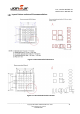
The proximity of ground vias must be close to the pad. (See Figure 9-1)
Signal traces must not be run underneath the module on the layer where the module is
mounted.