a module solution provider WS2116-A0 WS2116-F0 Ultralow Power Sub-1GHz and BLE Wireless MCU Module STM S2-LP with PA & BlueNRG-2 Solution Datasheet Draft 0.2 Prepared By Reviewed By Approved By ------------------------------------------------------------------------------------------------------------- ------------------------------------Copyright © JORJIN TECHNOLOGIES INC. 2018 http://WWW.JORJIN.COM.
DOC No: WS2116-A0A-DTS-D03 Index 1. OVERVIEW ....................................................................................................................................... 3 1.1. GENERAL FEATURES ........................................................................................................................ 3 1.2. MODELS FUNCTIONAL BLOCKS .......................................................................................................... 3 2. FUNCTIONAL FEATURES .....................
DOC No: WS2116-A0A-DTS-D03 5.2. DEBUG PORT ............................................................................................................................... 19 5.3. ANTENNA SELECTION GUIDE ........................................................................................................... 19 6. PACKAGE INFORMATION ............................................................................................................... 20 6.1. MODULE MECHANICAL OUTLINE .............................
DOC No: WS2116-A0A-DTS-D03 1. OVERVIEW The WS2116-A0 is a sub-1GHz with PA and Bluetooth® low energy ultralow power wireless MCU module. This module is built-in STM S2-LP and BlueNRG-2 chip. The module is a cost-effective, high performance, ultra-low power, sub-1GHz and Bluetooth® low energy RF devices. Very low active RF and MCU current and low-power mode current consumption provide excellent battery lifetime and allow for operation on small coin cell batteries and in energy-harvesting applications.
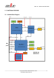
DOC No: WS2116-A0A-DTS-D03 2. FUNCTIONAL FEATURES 2.1. Module Block Diagram DIO pins WS2116-A0 WS2116-F0 WS2116-F0 only ____________________________________________________________________________________ Copyright © JORJIN TECHNOLOGIES INC. 2018 4 http://WWW.JORJIN.COM.
DOC No: WS2116-A0A-DTS-D03 2.2. Block Functional Feature BlueNRG-2: Bluetooth low energy wireless SOC Bluetooth low energy single mode system-on-chip compliant with Bluetooth 5.
DOC No: WS2116-A0A-DTS-D03 Air data rate from 0.
DOC No: WS2116-A0A-DTS-D03 3. MODULE OUTLINE 3.1. Signal Layout (Top View) ____________________________________________________________________________________ Copyright © JORJIN TECHNOLOGIES INC. 2018 7 http://WWW.JORJIN.COM.
DOC No: WS2116-A0A-DTS-D03 3.2. Pin Description Table 3-1. Pin Description Pin No.
DOC No: WS2116-A0A-DTS-D03 General purpose digital I/O of BlueNRG-2 21 DIO5 Digital I/O 22 DIO20 Digital I/O 23 DIO19 Digital I/O 24 DIO18 Digital I/O General purpose digital I/O of BlueNRG-2 25 DIO16 Digital I/O General purpose digital I/O of BlueNRG-2 26 DIO0 Digital I/O 27 DIO17 Digital I/O General purpose digital I/O of BlueNRG-2 28 DIO1 Digital I/O General purpose digital I/O of BlueNRG-2 29 DIO2 Digital I/O 30 DIO3 Digital I/O 31 GND GND 32 GPIO3 33 GND 34 VC
DOC No: WS2116-A0A-DTS-D03 POWER Power for SKY66420-11 47 VCC_PA2 48 GND GND GND 49 GND GND GND 50 SUB-1G RF 51 GND GND GND 52 GND GND GND 53 BLE RF 54 GND RF I/O RF I/O GND Sub-1GHz antenna port 2.4 GHz BLE antenna port GND ____________________________________________________________________________________ Copyright © JORJIN TECHNOLOGIES INC. 2018 10 http://WWW.JORJIN.COM.
DOC No: WS2116-A0A-DTS-D03 4. MODULE SPECIFICATIONS 4.1. Absolute Maximum Ratings Over operating free-air temperature range (unless otherwise noted) Pin Parameter MIN MAX Unit 15, 34 Power for BlueNRG-2 and S2-LP -0.3 +3.6 V 46, 47 Power for SKY66420-11 -0.3 +5.5 V 3, 4, 5, 6, 7, 8, 9, 10, 11, 12, 13, 17, DC voltage on digital input/output -0.3 +3.9 V 18, 19, 20, 21, 22, 23, 24, 25, 26, 27, pins -0.3 +3.
DOC No: WS2116-A0A-DTS-D03 4.4. Power Consumption Summary Ta = 25°C, VBAT=3.3 V, VCC_S2LP=3.3 V, VCC_PA = 3.3 V with internal DC-DC converter, unless otherwise noted. Test Conditions Parameter Reset Min Typ Max Units 5 nA Standby 500 nA Sleep mode: 32 kHz XO ON (24 KB retention RAM) 0.9 μA Sleep mode: 32 kHZ RO ON (24 KB retention RAM) 2.1 μA Active mode: CPU, Flash and RAM on 1.9 mA RX 8.8 mA BlueNRG-2 BLE TX +7 dBm 15.1 mA Supply current BLE TX +2 dBm 11.
DOC No: WS2116-A0A-DTS-D03 Sleep 5 nA 30.95 nA S2_LP Sleep (FIFOs retained) Supply current Ready 400 μA RX @ sensitivity level 8.5 mA TX CW @ 14 dBm(in boost mode) 25 mA TX CW @ 10 dBm(in boost mode) 16 mA Sleep Current 1 μA IVCC_ SKY66420-11 Transmit bypass mode 200 μA PA Supply current TX CW @ 27 dBm 280 mA 5 mA RX 4.5. 2.
DOC No: WS2116-A0A-DTS-D03 Sensitivity @ 920MHz, DR = 0.3 kbps, FDEV = 0.25 kHz, CHF = 1 kHz -128 dBm Low Gain Mode, DR = 1.2 kbps, FDEV = 1.2 kHz, CHF = 4 kHz -122 dBm 1% BER @ 2-GFSK BT = 0.5 DR = 38.4 kbps, FDEV = 20 kHz, CHF = 100 kHz -109 dBm DR = 100 kbps, FDEV = 50 kHz, CHF = 200 kHz -105 dBm Sensitivity @ 920MHz, DR = 4.8 kbps, DEV = 2.4 kHz, CHF = 10 kHz -114 dBm Low Gain Mode, DR = 9.6 kbps, DEV = 4.8 kHz, CHF = 20 kHz -112 dBm 1% BER @ 4-GFSK BT = 0.5 DR = 19.
DOC No: WS2116-A0A-DTS-D03 4.9. Internal 50MHz Crystal Oscillator ( for S2-LP ) over operating free-air temperature range (unless otherwise noted) Test Conditions Parameter Min Crystal frequency Typ Max Units 50 MHz Crystal frequency tolerance (1) Without initial frequency calibration -40 40 ppm Crystal frequency tolerance (2) Initial frequency is calibrated by software -20 20 ppm (1) Includes initial tolerance of the crystal, drift over temperature, aging ( 5 years ).
DOC No: WS2116-A0A-DTS-D03 IOL TC (VOL = 0.4V) 6.8 11.2 15.8 mA (High drive strength) TC1 (VOL= 0.42V) 7.6 13.2 20.1 mA TC2 (VOL =0.45V) 3.3 6 9.9 mA IOH TC (VOH = 2.4V) 5.5 10.6 17.6 mA (Low drive strength) TC1 (VOH= 1.72V) 3.7 7.2 12 mA TC2 (VOH =1.35V) 1.4 3 5.6 mA IOH TC (VOH = 2.4V) 9.9 19.2 31.7 mA (High drive strength) TC1 (VOH= 1.72V) 6.7 12.9 21.6 mA TC2 (VOH =1.35V) 2.4 5.5 10.1 mA 4.11.
DOC No: WS2116-A0A-DTS-D03 4.14. SKY66420-11 Gain vs. Pout Tc = 25°C, VCC_PA = 3.3 V 4.15. SKY66420-11 Current vs. Pout Tc = 25°C, VCC_PA = 3.3 V 4.16. More Characteristics If you need more detail characteristics, please visit STM and Skyworks web site. BlueNRG-2 https://www.st.com/content/st_com/en/products/wireless-transceivers-mcus-and-modules/bluetooth-b luetooth-low-energy/bluenrg-2.html S2-LP: http://www.st.com/content/st_com/en/products/wireless-connectivity/sub-1ghz-rf/s2-lp.
DOC No: WS2116-A0A-DTS-D03 5. DESIGN RECOMMENDATIONS 5.1. GPIO Usage of BlueNRG-2 Because the function of some pins has been used in the module internally. The other functions of these pins could not be defined. Please refer the below table.
DOC No: WS2116-A0A-DTS-D03 5.2. Debug Port The BlueNRG-1 embeds the ARM serial wire debug (SWD) port. It is two pins (clock and single bi-directional data) debug interface, providing all the debug functionality plus realtime access to system memory without halting the processor or requiring any target resident code. Pin functionality Pin Name Pin description SWCLK DIO9 SWD clock signal SWDIO DIO10 SWD data signal The Cortex-M0 subsystem of the BlueNRG-1 embeds two breakpoints and one watch point.
DOC No: WS2116-A0A-DTS-D03 6. PACKAGE INFORMATION 6.1. Module Mechanical Outline A Top View Side View Note: A: Typical: 2.8mm, Maximum: 3.0mm Unit: mm Tolerance: +/- 0.2mm ____________________________________________________________________________________ Copyright © JORJIN TECHNOLOGIES INC. 2018 20 http://WWW.JORJIN.COM.
DOC No: WS2116-A0A-DTS-D03 Unit: mm Bottom View Note: 1> Pad tolerance as +/-30um 2> Recommend pad layout size on PCB at least 0.9 mm as the picture on the right side. ____________________________________________________________________________________ Copyright © JORJIN TECHNOLOGIES INC. 2018 21 http://WWW.JORJIN.COM.
DOC No: WS2116-A0A-DTS-D03 6.2.
DOC No: WS2116-A0A-DTS-D03 7. SMT AND BAKING RECOMMENDATION 7.1. Baking Recommendation Baking condition: - Follow MSL Level 4 to do baking process. After bag is opened, devices that will be subjected to reflow solder or other high temperature process must be a) Mounted within 72 hours of factory conditions <30°C/60% RH, or b) Stored at <10% RH. Devices require bake, before mounting, if Humidity Indicator Card reads >10% If baking is required, Devices may be baked for 8 hrs. at 125 °C. 7.2.
DOC No: WS2116-A0A-DTS-D03 Note: (1) Reflow soldering is recommended two times maximum. (7) Add Nitrogen while Reflow process: SMT solder ability will be better. Stencil thickness: 0.1~ 0.13 mm (Recommended) Soldering paste (without Pb): Recommended SENJU N705-GRN3360-K2-V can get better soldering effects. ____________________________________________________________________________________ Copyright © JORJIN TECHNOLOGIES INC. 2018 24 http://WWW.JORJIN.COM.
DOC No: WS2116-A0A-DTS-D03 8. REGULATORY INFORMATION This section outlines the regulatory information for the following countries: United States Europe Japan 8.1. United States Federal Communications Commission Interference Statement This device complies with Part 15 of the FCC Rules.
DOC No: WS2116-A0A-DTS-D03 FCC RF Radiation Exposure Statement: This equipment complies with FCC radiation exposure limits set forth for an uncontrolled environment. This equipment should be installed and operated with minimum distance 20cm between the radiator & your body.
DOC No: WS2116-A0A-DTS-D03 8.2. Europe Hereby, Jorjin Technologies Inc. declares that the radio equipment type RF module is in compliance with Directive 2014/53/EU. The compliance has been verified in the operating frequency band of 2400 MHz to 2483.5 MHz, and 868.055MHz to 868.205MHz. Developers and integrators that incorporate the WS2116-A0 RF Module in any end products are responsible for obtaining applicable regulatory approvals for such end product.
DOC No: WS2116-A0A-DTS-D03 8.3. Japan The WS2116-A0 is certified as a module with type certification number. End products that integrate this module do not need additional MIC Japan certification for the end product. ____________________________________________________________________________________ Copyright © JORJIN TECHNOLOGIES INC. 2018 28 http://WWW.JORJIN.COM.
DOC No: WS2116-A0A-DTS-D03 9. HISTORY CHANGE Revision D 0.1 D 0.2 Date Description 2018/10/12 Product Preview 2019/03/04 BLE Max output power modify Update Table 4.4 of power consumption 2019/06/28 Update voltage limited and Sigfox maximum output power in Sigfox certification report. 2019/07/22 Update Sigfox RC5 certification power at page 14. 2019/08/12 Add Part 8 : REGULATORY INFORMATION 2019/0924 Modulation schemes modify 2019/10/08 Add more detail in Part 5.