85894_M&R_TA7650C_A 1
EC Declaration of Conformity available at: www.jotron.com Abbreviations and definitions ALARM Message by which the unit signals the occurrence of an event. The alarm is indicated by an audible tone and/or a message (or icon) on the display. APM Audio and PTT Modem. The APM is designed for use in applications, which requires long distance control of radios through a 4 or 2 wire leased lines.
LAN Local Area Network I.ED Light Emitting Diode. ORC Operators Remote Control. With the ORC it is possible to select frequencies, which are stored in the channel memory of the radio. To ease the operation, channel names can be used for each frequency. The ORC requires a separate line pair that is connected to the serial interface of the radio. Several ORC units may share the same line. PA Power Amplifier PSU Power Supply Unit. Separate unit to power the equipment.
Amendment Record AMENDMENT NO. INCORP. BY DATE PAGE(S) VERSION REASON FOR CHANGE 1 ES 21.05.10 26 PA New release 2 ES 26.05.
The information in this book has been carefully checked and is believed to be accurate. However, no responsibility is assumed for inaccuracies. Jotron AS reserves the right to make changes without further notice to any products or modules described herein to improve reliability, function or design. Jotron AS does not assume any liability arising out of the application or use of the described product. SAFETY INSTRUCTIONS CAUTION! This equipment contains CMOS integrated circuits.
TABLE OF CONTENTS 1 MAINTENANCE AND TROUBLESHOOTING.................................................................................... 1-1 1.1 ENVIRONMENTAL CHECK ...................................................................................................................... 1-1 1.2 ALARM READING .................................................................................................................................. 1-1 1.3 TX BITE MENU ......................................................
1 MAINTENANCE AND TROUBLESHOOTING 1.1 Environmental check Once a year: 1. 2. 3. 4. 5. 6. 7. Turn OFF the unit. Disconnect all plugs. Clean all metal surfaces using a humid rag to remove dirt and dust. Clean the knobs and connectors. Clean the loudspeaker cover. Connect all plugs. Turn ON the unit. 1.2 Alarm reading If for some reason the “AL” light lit red and the display show one of these conditions, please check TX BITE menu chapter 1.3 for abnormal readings.
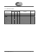
1.3 TX Bite menu To check the BITE alarm conditions, please see chapter 1.3.1 .
1.3.1 BITE alarm condition PARAMETER: PA_3V3 PA_5V PA_12V PA_28V PA_CUR MOD_6V MOD_LD_L01 PA_TEMP MOD_LEVEL_L01 PA_5VN PA_SWR Alarm criteria Min Max Unit 2.9 3.6 4.5 5.5 11 12.8 20 29 0 10 5.0 7.0 Digital 3v3 -25 +85 -20 8 -6.2 -4.0 NA NA V V V V A V °C dBm V - 85894_M&R_TA7650C_A Condition: PA current drain 3.
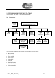
2 TECHNICAL DESCRIPTION TA-7650C The transmitter TA-7650C is described in this manual. 2.
2.2 Main module The main module consists of the main board and the modulator module. The modulator module is plugged into the main module. 2.2.1 Main board The main board consists of DSP section, Audio section, DAC/ADC interface, BITE interface, I/O interface, Ethernet controller and memory section. 2.2.1.1 DSP The heart of the board is a digital signal processor (DSP-IC42) running firmware for all interactions with it’s peripherals.
2.2.1.5 BITE interface The BITE interface consists of a A/D converter (IC 8) with 12 analog channels, reading analog measurements from all modules. It communicates with the DSP on a SPI bus. 2.2.1.6 I/O interface The I/O expander (IC12) provides the board with sufficient digital I/O lines for external and internal interfaces. It communicates with the DSP on a SPI bus. All external interfaces are passed through either relays or optocouplers for good immunity.
The signal then the first amplifier, Q6. Q6 is autobiased by the circuit consisting of Q3 and Q1. The gain in this stage is also adjustable by altering the bias of D1. This is part of the overall gain control in the PA. Then the signal is amplified further in the pre-driver, Q6. This is a MOSFET type transistor, and it is auto-biased by Q2 and Q4. The output is taken trough a 4:1 impedance transformer and fed to the input of the driver transistor Q8. Q108 is also of MOSFET type.
on-resistance MOSFET and acts as a switch when the input voltage goes below the wanted output voltage. IC6 supplies approx. 35V, (input voltage + 8.2V) to the main regulator circuit. The relay RL1 is the main powerswitch and also acts as a reverse polarity protection because of D4. Current measurement is done with IC2. There is also a current limiter (IC5B), which reduces supply voltage if current consumption is too high. IC8 generates -5VDC for the TX main board. 2.4.
prosessed in the DSP on the mainboard, and the I/Q signals to the modulator are modified accordingly. Synthesizer The VCO is operating at 2 times the output frequency. Q4 is the oscillator transistor and the frequency is controlled by varicaps D1and D2. The VCO have a separate regulated supply to get as low noise as possible on the output signal. The signal is then split up in three parts. On signal is going to the divider IC1 which supplies the modulator LO signal.
3 DIAGRAMS 3.
4 PARTS LIST Bill Of Material (BOM) Transmitter Unit BOM-84555 Front module Front board BOM-82419 BOM-84001 PA module PA board BOM-84554 BOM-84553 Reg.
5 APPENDIX 5.1 PSU-7002 bill of materials The PSU-7002 consists of a traded power supply, PBNO0311, from Powerbox A/S. The PBNO0311 consists of LEP240F-36 from Cosel.
85894_M&R_TA7650C_A 5-2
85894_M&R_TA7650C_A 5-3
85894_M&R_TA7650C_A 5-4
85894_M&R_TA7650C_A 5-5
85894_M&R_TA7650C_A 5-6
5.
5.2.
85894_M&R_TA7650C_A 5-9