
User's Manual


TIGO MD102AD User Manual
V1.01
2
Revised History
Date Revision Description
2011/08/17 1.0 1
st
Released
Table of Contents
1. Introduction .......................................................................................................... 3
1.1 Key Features ............................................................................................. 3
1.1.1 Module .............................................................................................. 3
1.1.2 Microcontroller ................................................................................ 3
1.2 Applications .............................................................................................. 3
2. Specifications ........................................................................................................ 4
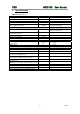
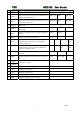
3. Pin Configurations ............................................................................................... 5
3.1 Pin Assignment ......................................................................................... 6
4. Additional Information ....................................................................................... 8
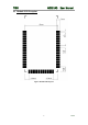
4.1 Outline Drawing ....................................................................................... 8
4.2 Module PCB Footprint ............................................................................ 9
4.3 Ordering / Lable Information ............................................................... 10
4.4 Tape and Reel Information ................................................................... 11
4.4.1 Tape Orientation and dimensions .................................................... 11
4.4.2 Cover tape details .............................................................................. 11
4.4.3 Leader and Trailer ............................................................................ 12
4.4.4 Reel Dimensions ................................................................................ 12
4.5 SMT IR Profile ....................................................................................... 13
4.6 How to Avoid ESD Damage to ICs ....................................................... 13
5. FCC Statement ................................................................................................... 14
6. IC Statement ....................................................................................................... 16