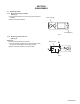
SERVICE MANUAL DVD/CD RECEIVER 5 2005 MA165 KD-AVX1 Area suffix J ------------- Northern America E ------------- Southern Europe A ------------------------ Australia UT ------------------------- Taiwan UN --------------------- Indonesia U -------------------- Other Areas KD-AVX1 OK DISP D SOURCE MENU T/P BACK BAND Lead free solder used in the board (material : Sn-Ag-Cu, melting point : 219 Centigrade) TABLE OF CONTENTS 1 2 3 4 5 PRECAUTIONS . . . . . . . . . . . . . . . . . . . . . . . . . . . . . .
SPECIFICATION for NORTHERN AMERICA version AUDIO AMPLIFIER SECTION Power Output 20 W RMS × 4 Channels at 4 Ω and [< or =] 1% THD+N Signal to Noise Ratio 80 dBA (reference: 1 W into 4 Ω) 4 Ω (4 Ω to 8 Ω allowance) Load Impedance Equalizer Control Range Frequencies 60 Hz, 150 Hz, 400 Hz, 1 kHz, 2.5 kHz, 6.3 kHz, 15 kHz Level ±10 dB 1.5 V/20 kΩ load Line-In Level/Impedance Line-Out Level/Impedance 5.0 V/20 kΩ load (full scale) Output Impedance 1 kΩ Subwoofer-Out Level/Impedance 2.
for EUROPE version AUDIO AMPLIFIER SECTION Maximum Power Output Front 50 W per channel Rear 50 W per channel Continuous Power Output (RMS) Front 20 W per channel into 4 Ω, 40 Hz to 20 000 Hz at no more than 0.8% total harmonic distortion. Rear 20 W per channel into 4 Ω, 40 Hz to 20 000 Hz at no more than 0.8% total harmonic distortion. 4 Ω (4 Ω to 8 Ω allowance) Load Impedance Equalizer Control Range Frequencies 60 Hz, 150 Hz, 400 Hz, 1 kHz, 2.5 kHz, 6.
for ASIA & AUSTRALIA version AUDIO AMPLIFIER SECTION Maximum Power Output Front 50 W per channel Rear 50 W per channel Continuous Power Output (RMS) Front 20 W per channel into 4 Ω, 40 Hz to 20 000 Hz at no more than 0.8% total harmonic distortion. Rear 20 W per channel into 4 Ω, 40 Hz to 20 000 Hz at no more than 0.8% total harmonic distortion. 4 Ω (4 Ω to 8 Ω allowance) Load Impedance Equalizer Control Range Frequencies 60 Hz, 150 Hz, 400 Hz, 1 kHz, 2.5 kHz, 6.
SECTION 1 PRECAUTIONS 1.1 Safety Precautions ! Burrs formed during molding may be left over on some parts of the chassis. Therefore, pay attention to such burrs in the case of preforming repair of this system. ! Please use enough caution not to see the beam directly or touch it in case of an adjustment or operation check. (No.
1.2 Preventing static electricity Electrostatic discharge (ESD), which occurs when static electricity stored in the body, fabric, etc. is discharged, can destroy the laser diode in the traverse unit (optical pickup). Take care to prevent this when performing repairs. 1.2.1 Grounding to prevent damage by static electricity Static electricity in the work area can destroy the optical pickup (laser diode) in devices such as CD players.
1.4 Important for laser products 5.CAUTION : If safety switches malfunction, the laser is able 1.CLASS 1 LASER PRODUCT 2.DANGER : Invisible laser radiation when open and inter lock failed or defeated. Avoid direct exposure to beam. 3.CAUTION : There are no serviceable parts inside the Laser Unit. Do not disassemble the Laser Unit. Replace to function. 6.CAUTION : Use of controls, adjustments or performance of procedures other than those specified here in may result in hazardous radiation exposure.
SECTION 2 SPECIFIC SERVICE INSTRUCTIONS This service manual does not describe SPECIFIC SERVICE INSTRUCTIONS. 1-8 (No.
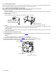
SECTION 3 DISASSEMBLY 3.1 Main body section 3.1.1 Removing the panel assembly (See Fig.1) (1) Push the button(detach) in the lower right part of the panel assembly. (2) Remove the panel assembly. Panel assembly Button(detach) Fig.1 3.1.2 Removing the side heat sink (See Fig.2) Reference: Remove the panel assembly as required. (1) From the left side of the main body, remove the two screws A and three screws B attaching the side heat sink. (2) Remove the side heat sink from the main body.
3.1.3 Removing the top chassis assembly (See Figs.3 to 6) • Remove the panel assembly and side heat sink. (1) From the top side of the main body, remove the two screws C attaching the top chassis assembly. (See Fig.3.) (2) From the back side of the main body, remove the two screws C attaching the top chassis assembly. (See Fig.4.) (3) From the both sides of the main body, remove the two screws C and screw D attaching the top chassis assembly. (See Figs.5 and 6.
3.1.4 Removing the front chassis assembly (See Fig.7) • Remove the panel assembly, side heat sink and top chassis assembly. (1) From the both sides of the top chassis assembly, remove the two screws E attaching the front chassis assembly. (2) Remove the front chassis assembly from the top chassis assembly. Top chassis assembly E E Front chassis assembly Fig.7 3.1.5 Removing the DVD mechanism assembly (See Figs.8 and 9) • Remove the panel assembly, side heat sink and top chassis assembly.
3.1.6 Removing the main sub board (See Fig.10) • Remove the panel assembly, side heat sink, top chassis assembly and DVD mechanism assembly. (1) From the top side of the DVD mechanism assembly, release the lock of the connector CN965 on the main sub board and disconnect the card wire. (2) Remove the two screws G attaching the main sub board on the DVD mechanism assembly and remove the main sub board.
3.1.10 Removing the connector board (See Figs.13 to 15) • Remove the panel assembly, side heat sink, top chassis assembly and front bracket assembly. (1) From the front side of the front bracket assembly, remove the two screws M. (See Fig.13.) (2) Remove the joints b and remove the detach lever from the front bracket assembly. (See Fig.13.) Reference: When attaching the detach lever, insert the end of the torsion spring in the hole c of the front bracket assembly. (See Fig.13.
3.1.11 Removing the main board (See Figs.16 and 17) • Remove the panel assembly, side heat sink, top chassis assembly, loading unit assembly and arm bracket assemblies (L)/(R). (1) From the back side of the main body, remove the screw P attaching the rear bracket. (See Fig.16.) (2) From the top side of the main body, take out the rod gear. (See Fig.17.) (3) (4) (5) (6) Reference: When attaching the rod gear, attach the washers with it as before. (See Fig.17.
3.1.12 Removing the rear bracket (See Fig.18) • Remove the panel assembly, side heat sink, top chassis assembly, loading unit assembly, arm bracket assemblies (L)/(R) and main board. (1) From the back side of the main board, remove the two screws Q attaching the rear heat sink. (2) Remove the three screws R, screw R' and screw S attaching the rear bracket. Reference: When attaching the screw R', attach the wire holder with it as before.
3.1.14 Removing the panel board (See Figs.20 and 21) • Remove the panel assembly. (1) From the back side of the panel assembly, remove the seven screws U attaching the rear cover to the panel assembly. (See Fig.20.) (2) From the inside of the rear cover, release the lock of the connector CN582 on the panel board and disconnect the card wire. (See Fig.21.) (3) Remove the five screws V attaching the panel board and take out the panel board from the rear cover. (See Fig.21.) 3.1.
3.2 DVD mechanism assembly 3.2.1 Removing the mechanism control board (See Fig.1) Caution: Before disconnecting the flexible wire extending from the DVD pickup, solder the short-circuit point on the flexible wire using a grounding soldering iron. If you do not follow this instruction, the DVD pickup may be damaged. (1) Turn over the body, and solder the short-circuit points on the flexible wire extending from the DVD pickup.
3.2.2 Removing the top cover (See Fig.2) (1) Remove the two screws D attaching the top cover on the back of the body. (2) Remove the top cover upward. Reference: When reassembling, set part b of the top cover under the bending part c of the chassis frame. 3.2.3 Removing the mechanism section (See Fig.2 to 4) • Remove the top cover. (1) From the bottom of the body, remove the screw E attaching the lug wire. (See Fig.2.) (2) Remove the two screws F attaching the right and left stoppers on the front side.
3.2.4 Removing the clamper unit (See Fig.5 to 7) • Remove the top cover and the mechanism section. (1) Remove the clamper2 spring on the bottom of the mechanism section. (See Figs.5.and 6.) (2) Release the part d of the clamper spring from the bending part of the chassis base assembly. (See Fig.7.) (3) Move the clamper unit in the direction of the arrow and turn. Release the two joints e and f, then remove the clamper unit upward. (See Fig.6.) Clamper2 spring 3.2.5 Reattaching the clamper unit (See Fig.
Clamper unit Clamper spring Fig.8 Clamper unit g Fig.9 1-20 (No.
3.2.6 Removing the front unit (See Fig.10 to 12) • Remove the top cover and the mechanism section. (1) Disconnect the flexible wire from connector CN202 on the mechanism control board at the bottom of the body. (See Fig.10.) (2) Remove the screw G attaching the front unit on the top of the body. (See Fig.11.) (3) Move the front unit toward the front to release joint h, and release two joints i and j on the right side of the chassis base assembly. Then remove the front unit upward. (See Figs.11 and 12.
3.2.7 Removing the loading arm assembly (See Fig.13 , 14) • Remove the top cover, the mechanism section and the front unit. (1) From the top of the body, move the loading arm assembly from the front side upward, and release the bosses from the right and left joints k and m of the chassis base assembly. (2) Release the boss from notch n of the connect arm on the right side of the body, and release the boss from notch p of the slide cam assembly on the left side. m Loading arm assembly n k Fig.
3.2.8 Removing the rod (L)(R)/roller assembly (See Fig.15 and 16) • Remove the top cover, the mechanism section, the front unit and the loading arm assembly. (1) Release the rod (L) and (R) from the joints q at the bottom of the loading arm assembly (See Fig.15.) (2) Remove the roller assembly from the loading arm assembly. (See Fig.16.) (3) Remove the two collars and washer from the roller assembly. (See Fig.16.
3.2.9 Removing the DVD pickup assembly (See Fig.17 to 19) • Remove the mechanism control board. (1) From the bottom of the body, turn the feed gear in the direction of the arrow to move the DVD pickup outwards. (See Fig.17.) (2) Remove the screw J attaching the thrust spring. (See Fig.17.) (3) Remove the DVD pickup assembly upward on the L.S.gear side and release from sub shaft at joint r. Move the lead screw of the DVD pickup assembly in the direction of the arrow to release from joint s. (See Fig.18.
3.2.10 Removing the spindle motor (See Fig.20) • Remove the mechanism control board. Remove the two screws L attaching the spindle motor on the bottom of the body. Spindle motor Caution: Perform adjustment when reattaching the spindle motor. L Fig.20 3.2.11 Removing the feed motor assembly (See Fig.21 and 22) • Remove the mechanism control board. (1) Remove the feed TRI. spring on the bottom of the body. (See Fig.21.) (2) Remove the two screws M attaching the feed motor assembly. (See Fig.21.
SECTION 4 ADJUSTMENT 4.1 (1) (2) (3) (4) (5) (6) (7) (8) 4.3 Test instruments required for adjustment Digital oscilloscope (100MHz) Jitter meter Digital tester Electric voltmeter Tracking offset meter Test Disc : VT501 or VT502 Extension studs : STDV001-3P Extension cable : EXTDV002-30P 4.2 Standard measuring conditions Power supply voltage Load impedance Line Output DC14.
4.4 Adjustment method for jitter After replacing the pickup, set the unit in the service mode to display a jitter value on the LCD. Confirm that the jitter value measured with a jitter meter is within 12% of the jitter value displayed on the LCD. If it is within 12%, then adjustment is not necessary. If the measured jitter value is outside the 12% tolerance range, perform the following adjustments. 4.4.1 Adjustment procedure (1) Connect each unit shown in Fig.1.
4.5 Jitter value conversion table Load the test DVD and set the unit to the service mode. A jitter value converted to the hex value is displayed on the LCD. Refer to the corresponding decimal notation value shown in the following Jitter Conversion Table. The adjustment is OK if the jitter value measured with a jitter meter is within 12% of the jitter value displayed on the LCD.
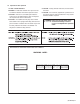
4.6 Service mode 4.6.1 Standard input/output conditions Power supply voltage Load impedance Line Output DC14.4V(11 to 16V) 4Ω(2 Speakers connection) 20KΩ 4.6.2 Service mode setting procedure (The DVD does not need to be loaded before starting the following procedure.) [STANDBY/ON ATTENUATOR] button [MENU] button [OK] button [EJECT] button [UP] button [VOLUME+/VOLUME-] button [B.SKIP] button [BACK] button [F.SKIP] button [DISPLAY] button [DOWN] button 4.6.3 Operation procedures 1.
2. Service mode 2 Keep this state more than 2 seconds while continuing pressing the [DISP] button, [VOLUME-] button and [EJECT] button sequentially. Screen indication SERVICE MODE2 INITIALIZE DVD SERVICE MODE 2 OK Press the [OK] button. Full initialization of EEPROM of a DVD unit (It is included a permanent domain) After clear completion, this indication is continued till an effective key is input. (OK ) 3.
A Screen indication SERVICE MODE VERSION AREA/REGION TEMPERATURE MEMORY CHECK DVD NTSC/PAL DVD CHECK MODE SERVICE MODE ERROR READ ERROR CLEAR Exchanging it operate a menu of a service mode with the [UP] button and [DOWN] button. Operate choice of a menu with a [OK] button. Return to previous menu with a [BACK] button.
B C ERROR READ DVD ERROR READ CD ERROR READ MECHA ERROR READ DVD ERROR READ E-1 : E04 : E-2 : E03 : E-3 : E02 : E05 : E01 : TOTAL : Reading of a DVD unit error history Reading of a history of an error stored in a DVD unit Indication of latest three error codes and first five error code Indication of total error count Error code Detailed error code CH ERROR READ E-1 : E04 : E-2 : E03 : E-3 : E02 : E05 : E01 : TOTAL : Reading of a CH changer error history Reading of a history of an error stored in a DVD u
4. Service mode 4 Keep this state more than 2 seconds while continuing pressing the [DISP] button, [BACK] button and [EJECT] button sequentially. Screen indication SERVICE MODE4 RDS S MODE MONITOR S MODE Exchanging it operate a menu of a service mode with the [UP] button and [DOWN] button. Operate choice of a menu with a [OK] button.
4.6.5 Error code tables Mechanism error code Error contents Error code Detailed error code Details Disc loading error B1 time out C1 time out D1 time out C2 time out B2 time out A2 time out F1 time out A0 (Switch state without existence) G1 time out Eject error F2 time out A1 time out B1 time out C1 time out D1 time out C2 time out B2 time out A0 (Switch state without existence) G2 time out Error in loading wait Loading of a running mode Disc was pulled out in a wait.
4.6.
4.6.8 Update method of firm ware Power on. Insert the disc which a farm was written in at. Screen indication VERSION UP DISC PROGRAM WRITING MODE CURRENT VERSION 0735 NEW VERSION 0795 READING... Current version Version to write in If "PLEASE EJECT" was displayed after the writing end, take out a disc. Close a panel and confirm a version.
4.6.9 Monitor adjustment When adjusting, switch on the main unit and insert a test disc (VT-501). And play the test disc and pause it. (Exit for VCO FREE-RUN adjustment) R/W CHROMA 1 1. Set the service mode 4. 2. Exchanging it operate a menu of a service mode with the [UP] button and [DOWN] button. 3. Change data with the [B.SKIP]/[F.SKIP] buttons. 4. Write data with a [OK] button.
SECTION 5 TROUBLESHOOTING 5.1 16 PIN CORD DIAGRAM [for E version] GN WH GN/BK WH/BK VI/BK GY/BK VI GY NC BR BL/WH L. GN RD OR/WH BK YL BK Black GN Green RD Red VI Violet BL Blue GY Gray WH White YL Yellow OR Orange Brown BR L.GN Light Green NC BR NC YL BL/WH OR/WH RD BK Choking Coil YL MEMORY YL RD RD ACC BR TEL BL/WH REMOTE OR/WH ILL BK GND VI RR+ VI/BK RR- GY FR+ GY/BK FR- WH FL+ WH/BK FL- GN RL+ GN/BK RD RL- L.
16 PIN CORD DIAGRAM [for A, J, U, UN, UT version] GN WH GN/BK WH/BK BK Black GN Green VI/BK GY/BK RD Red VI Violet VI GY BL Blue GY Gray BL BR WH White YL Yellow BL/WH L. GN OR Orange RD OR/WH BK YL BR GN RL+ WH FL+ GN/BK RL- WH/BK FL- VI/BK RR- GY/BK FR- VI RR+ GY FR+ BL ANT BL/WH REMOTE Brown Light Green POWER ANTENNA L.GN REMOTE OUT 5.2 TEL BR TEL MUTING ILL OR/WH ILLUMINATION CONTROL RD ACC BK GND YL MEMORY L.
Victor Company of Japan, Limited AV & MULTIMEDIA COMPANY CAR ELECTRONICS CATEGORY 10-1,1chome,Ohwatari-machi,Maebashi-city,371-8543,Japan (No.
PARTS LIST [ KD-AVX1 ] * All printed circuit boards and its assemblies are not available as service parts. Area suffix J ------------- Northern America E ------------- Southern Europe A ------------------------ Australia UT -----------------------------Taiwan UN ---------------------- Indonesia U -------------------- Other Areas - Contents Exploded view of general assembly and parts list (Block No.M1) DVD mechanism assembly and parts list (Block No.MJ) Electrical parts list (Block No.
Exploded view of general assembly and parts list Block No.
1 M M 114 114 114 114 114 114 125 120 8 133 126 h k 62 21 65 119 p 118 121 h 130 p n 127 128 k 34 n m q b 122 132 21 64 124 w r 66 70 18 a 9 108 123 17 68 69 t j 131 7 126 129 40 77 t c 46 39 21 44 45 43 42 71 Switch board f 77 Main board 117 50 41 s 11 g 52 41 47 104 106 m 38 31 110 75 30 80 76 76 52 54 53 48 36 52 35 36 12 24 78 37 111 74 78 73 74 34 80 49 112 28 d Panel switch board 55 52 75 26 31 51 52 101 106 q 79
General Assembly Block No. [M][1][M][M] 3-4 Symbol No. Part No.
Symbol No. Part No.
DVD mechanism assembly and parts list Block No. M J M M Grease FMU-JD4-2D = JVS-1003 = MOBIL-1 = JVG-31N = JC-803B = 1401C 18 14 18 93 97 94 95 15 96 BACK SIDE A 92 29 91 6 7 87 34 30 90 28 B 32 36 88 29 27 89 31 37 34 24 64 c 22 40 35 33 19 c 23 47 56 62 44 48 49 51 59 58 61 46 45 H K D AFTER SET PICK UP SA.
DVD mechanism Block No. [M][J][M][M] Symbol No. Part No.
3-8 Symbol No. Part No. Part Name 75 76 77 78 79 80 81 82 83 84 85 86 87 88 89 90 91 92 93 94 95 96 97 98 LV43010-001A LV43063-001A LV43011-001A QYSPSFT2040ZA LV33624-001A VKZ4539-056 LV21288-001A VKZ4539-056 LV43064-001A LV43065-001A LV43066-001A VKZ4730-002 LV21298-007A LV43070-001A LV43355-001A LV30225-0J6A LV21299-006A VKZ4539-056 LVB30012-001A NSW0187-001 NSW0187-001 NSW0187-001 VKZ4539-055 LV44232-001A L.S.GEAR L.S.
Electrical parts list Main board Symbol No. Part No.
Symbol No. Part No. Part Name Description Local C36 C37 C101 C102 C103 C104 C105 C106 C108 C109 C111 NCB31CK-223X QERF1HM-225Z NBE41AM-476X QERF1EM-475Z NDC31HJ-221X NDC31HJ-101X NDC31HJ-151X QERF1EM-475Z NDC31HJ-101X QERF1EM-475Z NCB31CK-223X C CAPACITOR E CAPACITOR TA E CAPACITOR E CAPACITOR C CAPACITOR C CAPACITOR C CAPACITOR E CAPACITOR C CAPACITOR E CAPACITOR C CAPACITOR 0.022uF 16V K 2.2uF 50V M 47uF 10V M 4.7uF 25V M 220pF 50V J 100pF 50V J 150pF 50V J 4.7uF 25V M 100pF 50V J 4.7uF 25V M 0.
Symbol No. Part No.
Symbol No. R231 R232 R233 R240 R241 R242 R243 R251 R252 R253 R254 R261 R262 R263 R264 R271 R272 R273 R281 R282 R283 R301 R302 R303 R315 R320 R321 R322 R323 R324 R325 R326 R327 R328 R329 R330 R331 R332 R333 R334 R335 R336 R337 R338 R339 R340 R341 R342 R343 R370 R371 R372 R373 R374 R375 R376 R377 R378 R701 R702 R703 R704 R705 R706 R707 R708 R709 R710 R711 R712 R713 R714 R715 R716 R717 R718 R719 R720 3-12 Part No.
Symbol No. R804 R805 R806 R807 R808 R810 R811 R812 R813 R814 R815 R816 R819 R821 R822 R823 R824 R825 R826 R828 R829 R830 R833 R834 R835 R836 R837 R839 R841 R842 R843 R844 R845 R847 R848 R849 R850 R851 R852 R853 R855 R856 R857 R858 R859 R861 R862 R863 R871 R872 R881 R891 R892 R893 R894 R895 R901 R902 R903 R913 R914 R915 R920 R921 R922 R923 R924 R925 R926 R927 R928 R929 R931 R932 R933 R934 R935 R936 Part No.
Symbol No. Part No.
Symbol No. C609 C611 C612 C613 C614 C615 C616 C617 C618 C619 C620 C621 C622 C623 C624 C625 C626 C630 C631 C633 C635 C636 C637 C638 C639 C645 C647 C649 C650 C651 C652 C653 C654 C655 C656 C657 C658 C659 C660 C661 C662 C663 C664 C665 C666 C667 C668 C669 C670 C671 C672 C673 C674 C675 C676 C677 C678 C679 C680 C681 C682 C683 C684 C685 C686 C687 C688 C689 C690 C691 C692 C693 C694 C695 C696 C697 C698 C699 Part No.
Symbol No. R472 R473 R474 R475 R476 R477 R478 R480 R481 R482 R483 R484 R485 R486 R487 R488 R489 R490 R491 R492 R493 R494 R495 R501 R502 R504 R505 R506 R507 R512 R513 R514 R515 R516 R517 R518 R519 R520 R521 R522 R523 R524 R525 R526 R527 R528 R529 R530 R531 R544 R545 R546 R547 R548 R549 R550 R551 R556 R573 R574 R575 R576 R577 R578 R579 R580 R581 R584 R585 R587 R588 R591 R593 R594 R596 R597 R598 R599 3-16 Part No.
Symbol No. Part No.
Symbol No. C202 C203 C204 C205 C206 C211 C212 C213 C221 C222 C251 C252 C253 C254 C255 C256 C257 C258 C259 C264 C265 C266 C267 C268 C301 C302 C305 C307 C308 C309 C310 C311 C312 C313 C314 C315 C316 C317 C318 C319 C320 C321 C322 C323 C324 C325 C326 C330 C331 C332 C333 C334 C335 C337 C338 C339 C340 C341 C347 C348 C349 C350 C351 C352 C356 C364 C365 C366 C369 C371 C380 C384 C391 C392 C393 C395 C396 C397 3-18 Part No.
Symbol No. R259 R260 R300 R301 R303 R306 R307 R308 R309 R310 R312 R313 R314 R315 R316 R317 R318 R319 R321 R322 R323 R325 R326 R327 R328 R329 R332 R333 R334 R335 R336 R337 R338 R339 R340 R345 R346 R347 R348 R349 R350 R351 R352 R353 R354 R355 R356 R357 R358 R359 R360 R361 R362 R363 R364 R365 R366 R370 R372 R373 R380 R384 R385 R386 R390 R391 R392 R393 R394 R396 R399 R401 R402 R403 R404 R411 R421 R422 Part No.
Packing materials and accessories parts list Block No. M 3 M M No additional / supplemental order of WARRANTY CARDs are available.
Packing and Accessories Block No. [M][3][M][M] Symbol No. Part No.
SCHEMATIC DIAGRAMS DVD/CD RECEIVER KD-AVX1 CD-ROM No.
Safety precaution ! Burrs formed during molding may be left over on some parts of the chassis. Therefore, pay attention to such burrs in the case of preforming repair of this system. ! Please use enough caution not to see the beam directly or touch it in case of an adjustment or operation check.
< MEMO >
Block diagram DVD servo control section LPCO2 CDLDCUR Q103 Q104 LD+ PICK UP F+,FT+,T- AOUTL+ AOUTLAOUTR+ AOUTR- IC301 DV2.
Main amplifier section FM/AM,SEEK,SD/ST,CFSEL,MRC PLLDI,PLLDO,PLLCK,PLLCE TU1 FM/AM TUNER W1 ANT FL,FR RL,RR CN961 CN966 IC321 E.VOLUME DVDL DVDR IC801 REGULATOR VOLDA VOLCK VOLMUTE SA_CLK SA_OUT DVDL,DVDR LRMUTE UCS,SCS SCLK U2SDT S2UDT CPURST COMPOSITE TX COMPOSITE VIDEO IN/OUT DIGITAL OUT 2nd AUDIO OUT & REVERSE GEAR SIGNAL OE REMOTE ACC REMOTE VOUT VIN IC921 VIDEO SW IC931 DZONE SW TX LRMUTE UCS,SCS SCLK U2SDT S2UDT CPURST DVDL DVDR IC301 2nd AUDIO E.
Standard schematic diagrams R215 47k C215 100p 22k C337 IC332 CD4053BPW-X R342 R338 22k 100p 4.7/25 C338 R337 IC331 NJM4565V-X C341 47k C115 LINE-L LINE-G LINE-R 0.001 R115 0.047 470 C315 R315 Main amplifier section R341 820 C339 0.1 220p TU1 * C335 R334 R335 C336 27k R336 0.033 4.7/25 68k 47/10 47/10 10k 10k R339 R340 0.01 NI IC322 NJM4565V-X C326 0.
DDGND B822 NI NQL79GM-220X Q822 RT1N141C-X Q820 NI B821 NI COMPOSITE DDGND R921 0 V-PANEL C921 1 330/6.3 150 C931 1 R926 R859 R817 NI * 1 C935 330/6.3 C934 75 CN901 QNZ0607-001 TEL R857 PARK R858 ILL R872 * 0 C152 C162 C362 C252 C262 100p 100p 0.022 100p 100p 100 100 CN361 QGA2501C1-07 R164 K871 * TP9 R936 * Q372 RT1P441C-X 100p 100p 0.
0.01 C635 0 GDC-HD 0 10k R621 R623 10k 10k R625 R622 1k R624 0 C636 0.1 NI 0.01 C637 R626 0.1 C638 R648 0.01 10k R627 C639 10k R628 IC601 R649 GDC-VD R583 Panel-A section MB87P2040PMT R601 120 C634 NI C633 0.01 C632 NI 120 R602 120 R603 C601 GDC-G R604 2.2 K603 22 NQR0022-005X C602 NI C603 NI C604 2.2 GDC-B R605 K604 22 NQR0022-005X R606 C605 IC511 2.7k 22/10 C606 2.2 GDC-R R607 K605 22 NQR0022-005X L601 0.
Parts are safety assurance parts. When replacing those parts make sure to use the specified one. SML310BA1T/HJ-X DIMMER Q404 SML-310LT/MN/-X RT1N141C-X Q402 2SA1530A/QR/-X Q406 RT1P141C-X R599 2SA1530A/QR/-X R466 560 R467 47k Q453 (SHEET 3) QGF0523F1-30W 2SA1530A/QR/-X 47k CN583 KEYIN 470k R468 S464 S455 R455 560 0 D415 1k NSW0246-001X S454 NSW0124-001X D5 MC2838-X 1k 2.7k R447 S459 S452 D6 0 B472 D414 3.
R6904 NI NI NI R6903 R6905 Panel-B section R6906 D6901 100k 470p C673 R670 R672 180k C674 220p 0 R673 1M 0.022 R669 100k 0.001 68k 47k NI R6902 R6907 R6901 0.1 10k C671 100p C670 0.01 C669 47/6.3 47k C6901 R671 330k C672 R679 Q656 2SC3928A/QR/-X R685 C675 22/6.3 C676 330 R674 C678 0.47 0.022 C677 3.3k 10k 4.7/6.3 D6653 Q651 2SC3928A/QR/-X R675 R676 R678 C681 RB160M-30-X 50/60 RGBCLK 0.01 10k 0.
UDZS5.6B-X UDZS5.6B-X CN581 QGZ2203M1-20X D581 D582 D583 D584 UDZS5.6B-X D585 D587 UDZS5.6B-X D586 UDZS5.6B-X UDZS5.6B-X NI RESET PS2 REMOCON KEYDATA DISPDATA TP656 TP666 ACC5V D6653 RB160M-30-X VIDEO (SHEET 4) DISPCE DISPCLK MIC0N3.3V R597 NI NI NI NI NI NI D589 D590 D591 D592 D593 D594 UDZS5.
2-9 NI C9002 NI C9006 C9001 NI C9005 NI NI C9004 C9007 NI NI 0 C9003 NI C9008 (SHEET 1) TO CN403 (SHEET 5) 220 R9012 0 R9013 0 R9011 (SHEET 3) R9001 QGB2027L8-30X CN966 Connecting section CN965 QGF0523F1-45W
CN964 CN963 QGF1038F1-20X (SHEET 1) QGZ2203L1-20X S896 CN892 QGF0523F1-07W NSW0183-001X S894 NSW0183-001X S893 NSW0183-001X S892 NSW0183-001X S891 (SHEET 1) NSW0183-001X S895 NSW0183-001X SHEET 4 2-10
DVD servo control section P3.3V K399 NQR0502-001X IC399 MA7 BA1 MA10 MA8 BA0 C309 0.1/16 MA11 MA9 NCSM NCAS MCK DQM0 NWE 27 0.1/16 0.1/16 C17 C18 DQM1 0.1/16 EXDAT3 0.1/16 C384 0.1/16 EXDAT11 NCAS MCK EXDAT10 47k C21 C398 /FL_RST R396 MDQ8 NI EXDAT4 NI NWE MDQ9 C394 MDQ7 NEXWE DQM0 MDQ10 C391 MDQ6 C19 EXDAT12 NRAS EXDAT5 DQM1 MDQ11 0.1/16 MDQ5 EXDAT13 EXADR20 R303 EXDAT6 EXADT8 EXADR19 C268 EXADT9 MDQ12 MDQ4 0.1/16 EXDAT14 0.
R300 0 IC303 R301 0 NI D3.3V R302 0 0 R356 R355 NI NI NI C303 NI C360 C361 NI C302 47/6.3 0.1/16 C305 NQR0502-001X C362 K301 EXDAT7 EXDAT9 EXDAT6 EXDAT10 EXDAT5 EXDAT11 EXDAT4 EXDAT12 EXDAT3 EXDAT13 EXDAT2 EXDAT14 EXDAT1 DQM3 EXDAT15 DQM2 EXDAT0 MA3 MA4 MA2 MA5 MA1 MA6 MA0 MA7 MA10 BA1 MA8 BA0 P3.3V D1.2V D3.3V IC302 47/6.3 C365 0.
Printed circuit boards Main board Lead free solder used in the board (material : Sn-Ag-Cu, melting point : 219 Centigrade) Forward side R719 C212 R211 R775 R784 R991 R992 R930 C732 R712 R711 IC731 C731 IC881 C924 C931 C921 C923 R929 IC921 R923 R123 C125 C126 R785 R933 R786 IC931 C966 R787 R788 C964 C826 C922 R703 R702 CN965 C9008 R9001 C9002 C9001 CN966 C9003 C9004 R9011 C9007 C9005 C9006 (Main sub board) 2-13 R18 TU1 R22 R21 R718 IC741 R920 R922 BZ951 C934 C933 C96
Reverse side IC912 IC801 CN901 CN361 R913 C343 C902 R915 R912 C373 IC371 C275 C372 C847 C848 R201 R303 R301 R101 C833 R816 R818 TP6 TP7 W4 IC811 L962 R960 C817 C967 C968 C831 C812 Q811 R967 R829 R839 Q822 R828 R813 R817 R819 R820 Q821 C826 L821 C837 C815 R814 R938 TP702 TP708 TP706 TP704 TP707 TP705 TP703 TP701 R377 R376 D821 C106 R202 C305 C101 R102 C102 C829 C836 R753 C964 C963 L826 L828 L827 C966 C965 K932 C813 L825 L824 C925 R939 R928 CN961 C933 C923 R9
D414 S451 2-15 R452 R453 S460 R596 Q402 Q403 D406 S459 R434 R435 R584 R582 D407 R436 R437 R438 D403 R413 R414 R415 R455 Q404 R431 R432 R433 R616 R617 R594 R459 Q401 R448 R583 B650 S454 S501 R6904 R6905 C6903 C699 TP663 TP683 L659 B654 TP666 D584 D586 D588 D590 R661 R660 TP665 TP685 D582 D583 D585 D587 D589 D591 D592 D593 D594 TP681 TP661 R693 R687 C667 TP684 TP664 B656 TP662 TP682 C695 L658 C650 Q693 R691 C697 B657 B651 B652 R692 Q691 Q692 C696 R686 C664 R662 C66
R680 C689 C687 C686 C685 C684 Q652 R682 D6901 C6901 R6902 L656 R6921 R618 C630 C631 R619 R620 C632 C633 C634 C624 C622 Q6602 C606 C6602 R532 C6601 C620 Q6601 R6601 L603 C581 C582 C583 R505 C604 C601 R6604 C6606 R589 K581 R556 R549 R548 R547 RA518 CN411 TP521 TP522 TP523 RA519 R6602 C6603 C6604 K602 Q6603 R6606 R6605 C507 C508 RA517 C618 C617 C615 C623 Q405 R449 R588 CN401 TP511 TP512 TP513 R470 C4006 C4007 RA512 RA513 L657 L652 C4004 C4003 IC511 RA511 R526 Q6651 C521
Connector board Lead free solder used in the board (material : Sn-Ag-Cu, melting point : 219 Centigrade) Forward side (Panel switch board) (Connector board) Reverse side (Connector board) CN963 CN964 (Panel switch board) S896 S894 S891 S895 S893 S892 CN892 2-17
< MEMO >
2-18 C211 C340 R312 R313 C349 C330 C337 C338 C332 C334 C333 C331 C335 C317 C491 R314 R315 C313 R316 C339 R321 Q103 C111 C104 C103 R101 C113 C23 R361 R21 C107 R113 C22 R305 R357 R358 R538 R537 R536 C531 R442 R441 R106 R116 R114 R105 K433 R345 K431 K430 K444 IC401 C305 R390 C18 R112 R111 R303 C20 R350 R360 C252 R491 R108 R107 R364 C359 R363 C358 Q101 C106 R104 R103 R125 C397 R355 R356 K426 K451 C302 R389 SW5 K405 K406 K403 K441 R331 K404 K452 C453 C380 C15 C21 R325
CN101 TP4 TP491 R205 C206 C205 TP1 TP51 IC 20 C251 C258 R256 R254 C602 R601 C601 R603 L302 TP36 C266 C256 TR /SPMUTE C362 C269 C603 SPDRV R602 TP39 C303 R332 R604 R365 C368 TP31 C341 C312 IC251 TP33 K311 TP457 R260 TP453 CN202 C365 C364 TP452 IC302 C367 TP436 TP435 C411 L-END SWGND R411 C412 C422 SW2 SW3 R257 R252 R208 R209 L602 TP444 TP455 R605 R606 L601 TP442 TP437 C401 LRCLK DCLK DDATA B203 C255 R307 R306 R369 B601 K601 TP37 X351 R317 TP448
Victor Company of Japan, Limited AV & MULTIMEDIA COMPANY CAR ELECTRONICS CATEGORY 10-1,1chome,Ohwatari-machi,Maebashi-city,371-8543,Japan (No.