KD-SH99R SERVICE MANUAL CD RECEIVER KD-SH99R Detachable ATT ANGLE EQ CD FM AM RD CH AUX SEL VOLUME RM-RK100 Area Suffix E ------- Continental Europe EX ----- Central Europe Contents Safety precaution Preventing static electricity Disassembly method Adjustment method Flow unit reading TOC of CD/CD-R/CD-RW Maintenance of laser pickup Replacement of laser pickup Description of major ICs COPYRIGHT 2001 VICTOR COMPANY OF JAPAN, LTD. 1- 2 1- 3 1- 4 1-15 1-18 1-20 1-20 1-21~45 No.49645 Jun.
KD-SH99R < Service mode > The menu in the service mode can be switched with UP/DOWN. The menu selected by the SEL button input is executed. The ordinary mode "UP" + "DOWN" + VR counterclockwise rotation. DEL EEPROM EEPROM data all clear (changer is connected). CH CH ERR CD changer error career call (changer is connected). DELL CH ERR CD changer EEPROM clear (EEPROM career) RUNNING CD CD running mode (Do not use in service). RUNNING SH Running mode of front panel (Do not use in service).
KD-SH99R Memory to EEPROM of 6 digits, 1st and 2nd digit are indicate the operation mode when occur the error, 3rd to 6th digit are indicate details of error. LCD indication time is use lower 2digits of details of error. This series is indicate ERR XX (XX is error code). When details of error is 0A0001 , it is indicate ERR 01, details of error is 0E0031 , it is ERR 31. Switch is from this side sequentially PSW1, PSW2,.....PSW6. Details of error 1.
KD-SH99R Description of major ICs UPD784215AGC146(IC701):MAIN CPU 1.Pin layout 75 51 76 50 100 26 1 25 2.
KD-SH99R UPD784215AGC146(1/2) Pin No. 1 2 3 4 5 6 7 8 9 10 11 12 13 14 15 16 17 18 19 20 21 22 23 24 25 26 27 28 29 30 31 32 33 34 35 36 37 38 39 40 41 42 43 44 45 46 47 48 49 50 1-22 Symbol PREQ AMUTE DIMMER-OUT ANT PEM VDD X2 X1 VSS XT2 XT1 RESET I/O O O O O O O O O I I RDS-SCK RDS-DA REMOCON AVDD AVREF0 SD-ST I O I I I I I I MRC DATA KEY0 KEY1 TEMP LEVEL SQ S.
KD-SH99R UPD784215AGC146(2/2) Pin No.
KD-SH99R UPD63711AGC(IC603):RF Servo amp 1.Pin layout 144 1 109 108 36 73 37 72 2.Pin function UPD63711AGC(1/3) Pin No. 1 2 3 4 Symbol VSSO ZRASO ZCASO ZCAS1 I/O O I I 5 VSSO I 6 ZOE I 7 8 9 ZUWE ZLWE VSSO O I I 10 11 12 13 14 15 16 17 18 19 20 21 22 23 24 25 26 27 RA0 RA1 RA2 RA3 RA4 RA5 RA6 RA7 VDD0 VSS0 RA8 IO0 IO1 IO2 IO3 IO4 IO5 VSSO O O O Function It is GND of the logic circuit. It is RFOK signal output terminal. Reset signal input terminal.
KD-SH99R UPD63711AGC(2/3) Pin No.
KD-SH99R UPD63711AGC(2/2) Pin No. 78 79 80 81 82 83 84 85 86 87 88 89 90 91 92 93 94 95 Symbol EQ2 EQ1 RF AGND A C B D F E AVDD REFOUT FE FEO TE TEO TE2 TEC I/O - Function Equalizer part connection terminal of RF amplifier. I I I I I I I O I O I O O I 96 97 AGND PD I 98 99 100 LD PN AVDD O I - Reversing input terminal of RF saming amplifier. It is GND of an analog circuit. Photo detector A input terminal. Photo detector B input terminal. Photo detector C input terminal.
KD-SH99R UPD70F3033AC015(IC606):SUB CPU 1.Pin layout 100 76 1 75 25 51 26 50 2.Pin function Pin No.
KD-SH99R UPD70F3033AC015(2/2) Pin No.
KD-SH99R MAS3507D-QG-G10 (IC806) :MP3 decoder PI12 SOI SOD SOC PI8 XVDD XVSS SID PI4 SIC SII 1.Pin layout 36 20 PI15 PI0 37 19 PI16 CLKO 38 18 PI17 PUP 39 17 PI18 WSEN 40 16 PI19 WRDY 41 15 RCS AVDD 42 14 PR CLKI 43 13 VSENS AVSS 44 4 5 6 7 8 12 9 10 11 DCSO RTW DCSG 3 POR 1 2 RTR PI1 EOD PI14 DCEN 21 VDD VSS 35 I2CD PI13 PI2 I2CC 33 32 31 30 29 28 27 26 25 24 23 34 22 TE PI3 (TOP VIEW) 2.
KD-SH99R 3.Pin function MAS3507D-QG-G10(1/2) Pin no.
KD-SH99R 3.Pin function MAS3507D-QG-G10(2/2) Pin no. Symbol I/O 36 PI1 IN/OUT 37 P0 IN/OUT 38 39 40 41 CLKO PUP WSEN ERDY O O I O 42 43 44 AVDD CLKI AVSS Supply I Supply 1) Function Start-up 1) : SDO Select 32 bit mode / 16 bit I 2 S mode Operation : MPEG header bit 30(Emphasis) Start-up 1) : Select Multimedia mode / Broadcast mode Operation MPEG header bit 31 (Emphasis) Clock Output (normal 24.576 MHz) Power Up, i.e.
KD-SH99R LC895199K-ND2(IC601):CD-ROM decoder 1.Pin layout 144 1 109 108 36 73 37 72 2.Pin function Pin No.
KD-SH99R LC895199K-ND2(2/3) Pin No.
KD-SH99R LC895199K-ND2(3/3) Pin No. 110 111 112 113 114 115 116 117 118 119 120 121 122 123 124 125 126 127 128 129 130 131 132 133 134 135 136 137 138 139 140 141 142 143 144 1-34 Symbol DAO ZPDIAG DA1 ZIOCS16 HITRQ ZDMACK VSS1 IORDY ZDIOR ZDIOR DMARQ VSS1 DD15 DDO DD14 DD1 VDDO VSS1 DD13 DD2 DD12 DD3 VSS1 DD11 DD4 DD10 VSS1 VDD0 DD5 DD9 DD6 VSS1 DD8 DD7 VDD1 Function ATAPI data bus ATAPI data bus ATAPi data bus ATAPi control signal ATAPI control signal 5.
KD-SH99R HA13164 (IC961) : Regulator MEMORY 1.Pin layout 1 2 3 4 5 6 7 8 9 10 11 12 13 14 15 2.Block diagram +B C1 100u C2 0.1u ACC VCC 8 3 ACC BATT.DET OUT 9 ANT OUT 2 Surge Protector C3 0.1u EXT OUT 1 BIAS 6 TSD COMPOUT C4 0.1u 4 ANT CTRL VDD OUT 7 CTRL CD OUT C7 0.1u 11 5 SW5VOUT 12 C5 0.1u AUDIO OUT ILMOUT 10 14 C8 0.1u C6 10u 15 GND 13 R1 ILM AJ UNIT R: C:F note1) TAB (header of IC) connected to GND 3.Pin function Pin No.
KD-SH99R LC75878W (IC501) : LCD driver 1. Pin layout 100 ~ 76 1 75 ~ ~ 25 51 COMMON DRIVER GENERAL PORT SEGMENT DRIVER & LATCH CONTROL REGISTER CLOCK GENERATOR OSC S1 COM8 COM1 P4 P1 2. Block diagram S75/COM9 S74/COM10 S73 26 ~ 50 VLCD CONTRAST ADJUSTER SHIFT REGISTER VLCD0 VLCD1 CCB INTERFACE VLCD2 VLCD3 CE CL DI INH VLCD4 VDD VSS 3. Pin function No.
KD-SH99R M61508FP-X (IC911) : E. volume 1. Pin layout & Block diagram 36 35 34 33 32 31 30 29 28 27 50K 26 25 24 23 22 21 20 19 LOUDNESS VDO (Digital) + VCC (Anarog) 3BAND TONE CONTROL (BASS/MID/TREBLE) Soft select REF A B B Zero detect Select SW I/F 12dB Z E R O C RO S S D E T E C TO R 12dB Z E R O C RO S S D E T E C TO R A TIMER DETECTOR LOUDNESS + 3BAND TONE CONTROL (BASS/MID/TREBLE) 1 2 3 4 2. Pin function Pin No.
KD-SH99R IN5- IN5+ IN4+ IN4- OUT4 MUTE2 SS,GND VREF VREFO OUT5 MUTE1 VM5- IN2+ VM3+ VM5+ VM3- VM1+ IN2- N.C VM1- VM4- IN3+ OUT1 OUT2 Vm2 IN1- VM4+ VBS2 Vm1 VM2- IN3- VBS1 VM2+ OUT3 IN1+ GND CH3IN REG+ REGB 1.Pin layout GND M63008FP-X (IC604) : 5ch Actuator driver 2.
KD-SH99R 28 15 1 14 2. Block diagram BCK Serial LBCK Input DATA I/F Vcc2R AGND2R 1.
KD-SH99R SAA6579T-X(IC51):RDS 1.Pin layout QUAL 1 16 RDCL RDDA 2 15 T57 Vref 3 14 OSCO MUX 4 13 OSCI VODA 5 12 V0DD VSSA 6 11 VSSD CIN 7 10 TEST SCOUT 8 9 MODE 2.
KD-SH99R BA3220FV-X (IC301,IC401) : Line out amp 1.Pin layout 14 8 3220 1 7 2.
KD-SH99R IS41C16256-35T(IC602):RAM 1.Pin layout 44 21 1 22 2.Block diagram OE WE LCAS UCAS CAS CLOCK GENERATOR WE CONTROL LOGICS CAS WE OE CONTROL LOGIC OE DATA I/O BUS COLUMN DECODERS SENSE AMPLIFIERS A0-A8 1-42 ADRESS BUFFERS ROW DECODER REFRESH COUNTER MEMORY ARRAY 262.
KD-SH99R IC-PST9333U-X (IC702) : Reset IC 1. Pin layout 2. Block diagram NC 1 NC 4 Vcc GND 2 GND 3 VOUT Vcc NC 4 1 3 VOUT 2 GND 3. Pin function Pin No.
KD-SH99R NJM4565V-X (IC171,IC951,IC323) : Ope amp 1. Pin layout & Block diagram 2. Pin function Pin No. 8 1 2 A 1 2 3 4 5 6 7 8 7 B 3 6 4 8 Function A output A-input A+input VB+input B-input B output V+ NJM4580V-X (IC801) : CD LPF 1. Pin layout & Block diagram 1 2 2. Pin function 8 A 7 B 3 6 4 8 Pin No. Function 1 2 3 4 5 6 7 8 A output A -input A +input VB +input B -input B output V+ RPM6938-SV4 (IC561) : Remote sensor 1.
KD-SH99R S-81332HG-KC-X (IC804) : Regulator 2. Block diagram 1. Pin layout 1 2 3 Vout GND Vin VIN 3 VREF 1 VOUT 1 2 3 2 GND LB1830M-X(IC608):Regulator 2.Block diagram 1.Pin layout OUT1 Vs OUT2 IN2 IN1 Vm Vm1 Vcont 10 9 8 7 6 VCC 1 2 3 4 5 Vcc OUT2 GND OUT1 Vs Vref Logic Predriver GND IN1 IN2 Vm Vcont Vref TC74VHC126FT-X(IC605):Buffer 1.Pin layout 2.
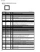
KD-SH99R Electrical parts list (Main board) A 3-8 Item Parts number Parts name BZ791 QAN0009-001Z C 1 NCB31EK-473X C CAPACITOR C 2 QERF1CM-476Z E CAPACITOR C 3 NCB31HK-103X C CAPACITOR C 4 QERF1CM-476Z E CAPACITOR C 5 QERF1AM-107Z C 7 Block No. 01 Remarks BUZZER Area A Item Parts number Parts name Remarks C 306 QERF1EM-475Z E CAPACITOR 4.7MF 20% 25V C 307 QERF1AM-107Z E CAPACITOR 100MF 20% 10V C 308 QERF1EM-475Z E CAPACITOR 4.
KD-SH99R Electrical parts list (Main board) A Item C 634 Parts number Parts name Block No.
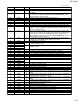
KD-SH99R Electrical parts list (Main board) A A A 3-10 Item Parts number Parts name C 986 NCB21EK-104X C CAPACITOR C 990 NCS31HJ-101X C CAPACITOR C 991 NCS31HJ-101X C CAPACITOR C 992 NCS31HJ-101X C 993 NCS31HJ-101X C 994 C 995 Block No.
KD-SH99R Electrical parts list (Main board) A Item Parts number Parts name Block No.
KD-SH99R Electrical parts list (Main board) A 3-12 Item Parts number Parts name Block No.
KD-SH99R Electrical parts list (Main board) A Item Parts number Parts name Block No.
KD-SH99R Electrical parts list (Front board) A 3-14 Item Parts number Parts name Block No.
KD-SH99R Electrical parts list (Front board) A Item Parts number Parts name S 510 NSW0066-001X TACT SWITCH S 511 NSW0066-001X TACT SWITCH S 512 NSW0066-001X TACT SWITCH S 513 NSW0066-001X TACT SWITCH S 514 NSW0066-001X TACT SWITCH S 515 NSW0066-001X TACT SWITCH S 516 NSW0066-001X TACT SWITCH S 517 NSW0066-001X TACT SWITCH S 518 NSW0066-001X TACT SWITCH S 591 NSW0146-001X DETECT SWITCH S 592 NSW0146-001X DETECT SWITCH S 593 NSW0146-001X DETECT SWITCH S 594 NSW0146-00
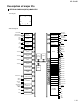
KD-SH99R Block diagram Mai amp section J1 TUL,TUR TU1 TUNER PACK ANT MUX CD servo section IC602 RAM LOADING MOTOR RA0 RA8 IO0 IO15 LC,UC,OE,WE,RA FEED MOTOR REST SWITCH CN601 SPINDLE MOTOR VOUTL, IC802 D/A CONVERTER VOUTR A,B,C,D,E,F, LD,PD BCK,LRCK,SDATA,C2PO REST SW1,SW2,SW3,SW4 SPD FEED TRD FOD CN703 OUT1 OUT2 IC701 MAIN CPU IC803 DAC SW RDSDA RDSCK IC911 E.VOL FRONT.R REAR.R IC941 POWER AMP IC401 LINE AMP FRONT.R REAR.R LINE.L LINE.
KD-SH99R Standard schematic diagrams KD-SH99R D161 0.047 1SS355 270k 0.22/50 C164 D162 390 R165 R164 1k 22k R161 1/50 47k IC941 TA8273H Q161 2SD601A QAU0203-001 1SS355 C161 C163 12k R167 TU1 R162 180k R163 Main amp section L1 QAM0105-002 NI C41 NI R111 C42 NI 220k C43 NI 220k R166 R211 C162 22/16 C40 D111 MA152WK TU.L CH.R R218 3.3k CD.R C210 1/16 C212 1/50 0.
KD-SH99R R811 33k R812 12k R813 IC801 CN601 QGB2027M2-26X LD SW4 R815 0.1 TP621 WE LRCK C633 0.1 SDATA SD3 IC601 C614 0.1 RA8 LC895199K-ND2 IO0 IO2 PD C2PO SA5 IO4 SA4 IO5 SA3 TP609 TP608 RD 15K 15K R817 C804 100/10 BCK 150 X601 QAX0599-002Z 200 0.1 C841 GND TP640 TP638 SI SO SCK STB NQR0007-003X NI C609 10/10 C604 0.1 R605 LRCK 3.3k 0.1 R606 7.5k R603 10k C603 C613 0.
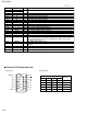
2 A R561 R562 RPM6938-V4 10k C561 4.7/6.3 47 B Q541 DTC114EKA-X 2.2k C 2-4 D E SEG25 SEG24 SEG23 SEG22 SEG21 SEG20 SEG19 SEG18 SEG17 R546 SEG16 3.3k SEG15 R565 SEG14 4.7/6.3 SEG13 3.3k SEG12 R564 SEG11 3.3k SEG10 D574 R531 2.
1 A Note:1016803A1_LVS10168-003A_1/1 B C C17 R13 100 D C25 R9 C24 0.01 R19 1k E R-CH C340.068 R23 100 C55 0.022 CF4 IC1 LA17000M C29 0.01 F 1 R45 4.7k C105 C57 X1 10.25MHz R31 5.6k C43 0.22 C49 VR1 R32 10k 50k C103 100 1 C65 1 C44 C46 1000p C45 1 R35 33k C102 1 0.01 C50 R38 1k R37 0 C47 R27 47k R26 0 C40 0.47 100p C3715p R201.8k C66 100p L7 C42 0.1 R33 8.2k 1 R36 56k R40 6.8k 1 L-CH C51 R41 8.2k R42 5.6k C522200p C530.022 C54 1 C104 2.