HARDWARE REFERENCE GUIDE Date : 28 November 2005 Doc. no. : C6713CPU_HRG Iss./Rev : 1.1 Page :1 Hardware Reference Guide micro-line® C6713CPU High performance DSP / FPGA board Orsys Orth System GmbH, Am Stadtgraben 25, 88677 Markdorf, Germany http://www.orsys.
HARDWARE REFERENCE GUIDE ® MICRO-LINE C6713CPU Date : 28 November 2005 Doc. no. : C6713CPU_HRG Iss./Rev : 1.1 Page :2 Contents 1 PREFACE...................................................................................................................... 6 1.1 Document Organization ......................................................................................................... 6 1.2 Documentation Overview .........................................................................................
HARDWARE REFERENCE GUIDE ® MICRO-LINE C6713CPU Date : 28 November 2005 Doc. no. : C6713CPU_HRG Iss./Rev : 1.1 Page :3 3.3 Internal fast SRAM ............................................................................................................... 21 3.4 DSP Peripherals ................................................................................................................... 21 3.5 External SDRAM ...........................................................................................
HARDWARE REFERENCE GUIDE ® MICRO-LINE C6713CPU 7.2.3 7.2.4 7.2.5 7.2.6 7.2.7 Date : 28 November 2005 Doc. no. : C6713CPU_HRG Iss./Rev : 1.1 Page :4 Configuring for HPI or McASP1 Usage ............................................................................... 47 Configuring micro-line® Pin D30 Termination ...................................................................... 47 Configuring for I2C interface #0 Operation ..........................................................................
HARDWARE REFERENCE GUIDE ® MICRO-LINE C6713CPU Date : 28 November 2005 Doc. no. : C6713CPU_HRG Iss./Rev : 1.1 Page :5 List of Tables Table 1: Memory map of the processor........................................................................................... 20 Table 2: Memory map of the C6713CPU ........................................................................................ 21 Table 3: default initialization values for the FPGA related CE space registers ...............................
HARDWARE REFERENCE GUIDE ® MICRO-LINE C6713CPU Date : 28 November 2005 Doc. no. : C6713CPU_HRG Iss./Rev : 1.1 Page :6 1 Preface This document describes the hardware of the C6713CPU board. It is intended to get an overview of the board and its features. Detailed information about programming, usage of the FPGA and the DSP is described in other documents that will be referenced throughout this document. 1.
Date : 28 November 2005 Doc. no. : C6713CPU_HRG Iss./Rev : 1.1 Page :7 HARDWARE REFERENCE GUIDE ® MICRO-LINE C6713CPU Configuration parameters, function names, path names and file names are written in italic typeface. Example: dev_id Source code examples are given in a small, fixed-width typeface. Example: int a = 10; Menus and commands from menus and submenus are enclosed in double-quotes. Example: Create a new project using the "Create Project..." command from the "File" menu.
HARDWARE REFERENCE GUIDE ® MICRO-LINE C6713CPU 1.5 Revision History Revision 0.1 0.5 0.9 1.0 1.1 Date : 28 November 2005 Doc. no. : C6713CPU_HRG Iss./Rev : 1.1 Page :8 Changes ORSYS internal preliminary version / April 2005 First public preliminary version / May 2005 Completely revised. Block diagram completed. Flash File System: short description only, reference to separate user's guide. Mentioned that HPI usage requires FPGA.
HARDWARE REFERENCE GUIDE ® MICRO-LINE C6713CPU Date : 28 November 2005 Doc. no. : C6713CPU_HRG Iss./Rev : 1.
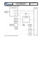
HARDWARE REFERENCE GUIDE ® MICRO-LINE C6713CPU 2.1 Block Diagram of the C6713CPU Figure 1: Block diagram of the C6713CPU Date : 28 November 2005 Doc. no. : C6713CPU_HRG Iss./Rev : 1.
HARDWARE REFERENCE GUIDE ® MICRO-LINE C6713CPU flash memory Date : 28 November 2005 Doc. no. : C6713CPU_HRG Iss./Rev : 1.
HARDWARE REFERENCE GUIDE ® MICRO-LINE C6713CPU 2.2 Date : 28 November 2005 Doc. no. : C6713CPU_HRG Iss./Rev : 1.1 Page : 12 Connectors 2.2.1 micro-line® Connectors The micro-line® connectors are the main I/O connectors of the C6713CPU. They provide access to all signals that are needed for a wide range of I/O connectivity.
HARDWARE REFERENCE GUIDE ® MICRO-LINE C6713CPU Date : 28 November 2005 Doc. no. : C6713CPU_HRG Iss./Rev : 1.1 Page : 13 interfacing over for the majority of the micro-line® connector pins. The user is no longer restricted to a fixed I/O logic.
HARDWARE REFERENCE GUIDE ® MICRO-LINE C6713CPU Date : 28 November 2005 Doc. no. : C6713CPU_HRG Iss./Rev : 1.1 Page : 14 can be software reconfigured by PLL settings. It can also be generated by the FPGA, allowing any clock frequency up to 100 MHz. Compared to the internal fast SRAM of the DSP chip, the on-board SDRAM is significantly slower. Therefore it is strongly recommended to use the internal memory of the DSP whenever it is possible.
HARDWARE REFERENCE GUIDE ® MICRO-LINE C6713CPU Date : 28 November 2005 Doc. no. : C6713CPU_HRG Iss./Rev : 1.1 Page : 15 DSP-internal temperature is roughly 15 degrees Celsius above the temperature measured by the sensor. Software drivers for the temperature sensor are included in the development kits, see [20] for details. Further information can be found in [18]. The temperature sensor is connected to the PLD by a separate I2C interface. It does not use the I2C interfaces of the DSP.
HARDWARE REFERENCE GUIDE ® MICRO-LINE C6713CPU Date : 28 November 2005 Doc. no. : C6713CPU_HRG Iss./Rev : 1.1 Page : 16 2.4.1 User Programmable LED's (PLD) These LED's are controlled by PLD registers (see chapter 3.10). They can be switched on and off by application software to display certain events or states.
HARDWARE REFERENCE GUIDE ® MICRO-LINE C6713CPU • • • Date : 28 November 2005 Doc. no. : C6713CPU_HRG Iss./Rev : 1.1 Page : 17 CE0 is used for on-board SDRAM CE1 is used for on-board flash memory , PLD and FPGA registers. CE2 and CE3 are used for the FPGA Please refer to chapter 3 for further descriptions of the CE spaces and their address ranges. 2.5.3 Inter Integrated Circuit (I2C) Interfaces The TMS320C6713 DSP provides two I2C interfaces.
HARDWARE REFERENCE GUIDE ® MICRO-LINE C6713CPU Date : 28 November 2005 Doc. no. : C6713CPU_HRG Iss./Rev : 1.1 Page : 18 2.5.6 Timers The TMS320C6713 DSP provides two independent 32-bit general purpose timers. The timers support two signaling modes and can be clocked by an internal or an external source. Each timer has a separate input pin and an output pin.
HARDWARE REFERENCE GUIDE ® MICRO-LINE C6713CPU Date : 28 November 2005 Doc. no. : C6713CPU_HRG Iss./Rev : 1.1 Page : 19 2.5.9 DMA The TMS320C6713 DSP provides an enhanced DMA (EDMA) controller with 16 channels and 16 possible synchronization events. It can be used to transfer data between two locations anywhere in the address range of the C6713CPU. EDMA transfers can be triggered by software, internal events, such as timers or serial ports, or by hardware interrupt lines.
HARDWARE REFERENCE GUIDE ® MICRO-LINE C6713CPU Date : 28 November 2005 Doc. no. : C6713CPU_HRG Iss./Rev : 1.1 Page : 20 3 Memory Maps and Description of the PLD Registers 3.1 TMS320C6713 Memory Map The memory map of the TMS320C6713 is divided into several sections: • • • internal memory DSP peripherals EMIF CE spaces CE0 .. CE3 The external devices are located at different CE (Chip Enable) spaces. The EMIF bus timing of each CE space can be individually set up.
HARDWARE REFERENCE GUIDE ® MICRO-LINE C6713CPU 3.2 Date : 28 November 2005 Doc. no. : C6713CPU_HRG Iss./Rev : 1.
HARDWARE REFERENCE GUIDE ® MICRO-LINE C6713CPU 3.7 Date : 28 November 2005 Doc. no. : C6713CPU_HRG Iss./Rev : 1.1 Page : 22 Endianness When data is transferred between the C6713CPU board and external hardware over the microline® connector it is important to know how data is stored in memory. The C6713CPU is configured for little endian operation. This means, less significant bytes are stored first (at lower addresses).
HARDWARE REFERENCE GUIDE ® MICRO-LINE C6713CPU 3.8 Date : 28 November 2005 Doc. no. : C6713CPU_HRG Iss./Rev : 1.1 Page : 23 EMIF Configuration All accesses to off-DSP-chip peripherals, such as on-board SDRAM, the UART or the FPGA are performed by the DSP's external memory interface (EMIF). The timings and interface type for these accesses can be software-programmed separately for each CE space (see Table 2 for an overview of the CE space usage). 3.8.
Date : 28 November 2005 Doc. no. : C6713CPU_HRG Iss./Rev : 1.
Date : 28 November 2005 Doc. no. : C6713CPU_HRG Iss./Rev : 1.1 Page : 25 HARDWARE REFERENCE GUIDE ® MICRO-LINE C6713CPU CPUSPEED: This bit can be used by application software to determine the DSP speed version and to program the DSP's PLL accordingly. CPUSPEED CPU clock frequency 0 225 MHz 1 300 MHz FLASH_A19: This bit represents the highest address line of the flash memory. When FLASH_A19 is 0 the lower 1 MB of the flash memory is selected.
Date : 28 November 2005 Doc. no. : C6713CPU_HRG Iss./Rev : 1.1 Page : 26 HARDWARE REFERENCE GUIDE ® MICRO-LINE C6713CPU 7 6 5 4 RED_LED GREEN_LED r, w, 00 r, w, 11 RED_LED: RED_LED 002 012 others 3 0 RESERVED Encoding off on reserved GREEN_LED: RED_LED Encoding 002 off 012 on 102 on when CE1 active, that is when Flash, PLD or FPG registers are accessed 112 on when Flash is accessed 3.10.
Date : 28 November 2005 Doc. no. : C6713CPU_HRG Iss./Rev : 1.1 Page : 27 HARDWARE REFERENCE GUIDE ® MICRO-LINE C6713CPU 7 6 5 4 SDA_STAT SDA_CTL SCL_STAT SCL_CTL r, 1 r, w, 1 r, 1 r, w, 1 3 0 RESERVED SDA_STAT: retrieves the current state of the SDA line. If this bit is read as 1, the SDA line is in a logic high state and no device pulls the line low. If 0 is read from this bit, the SDA line is pulled low by either the PLD (SDA_CTL bit), or the temperature sensor.
HARDWARE REFERENCE GUIDE ® MICRO-LINE C6713CPU Date : 28 November 2005 Doc. no. : C6713CPU_HRG Iss./Rev : 1.1 Page : 28 WDG_RST: The WD_RST pin of the PLD is connected to the watchdog input of the reset generator. If the watchdog is enabled the WD_RST pin must be set to 1 at least once per second. This must be done by writing a 1 to the WDR_RST bit of this register. The WDR_RST bit is self-clearing.
HARDWARE REFERENCE GUIDE ® MICRO-LINE C6713CPU Date : 28 November 2005 Doc. no. : C6713CPU_HRG Iss./Rev : 1.1 Page : 29 4 Boot Process and Default Setup of the C6713CPU After reset or power up the C6713CPU boots the Flash File System from flash memory. The Flash File System first checks, if a command from a host PC on the RS-232 interface is pending. If a command is pending, if performs the desired function (see [24]).
HARDWARE REFERENCE GUIDE ® MICRO-LINE C6713CPU Date : 28 November 2005 Doc. no. : C6713CPU_HRG Iss./Rev : 1.1 Page : 30 5 Using the Flash File System The Flash File System of the C6713CPU consists of three parts: • • • A target-resident boot loader which initializes the C6713CPU at startup, looks for commands on the RS-232 interface and then either loads auto-boot FPGA(s) / application or loads a Flash File System command executable over RS-232.
HARDWARE REFERENCE GUIDE ® MICRO-LINE C6713CPU Date : 28 November 2005 Doc. no. : C6713CPU_HRG Iss./Rev : 1.1 Page : 31 6 Description of the micro-line® Board Connectors 6.1 Location of the Connectors For the micro-line® connectors, Pin 1 is marked by a black square in Figure 6.
HARDWARE REFERENCE GUIDE ® MICRO-LINE C6713CPU 6.2 Date : 28 November 2005 Doc. no. : C6713CPU_HRG Iss./Rev : 1.1 Page : 32 Connector Overview Table 10 gives an overview about usage of the micro-line® connectors, including the 'classic' usage as peripheral interface as used with previous CPU boards. The classic peripheral interface is implemented in the micro-line® busmaster BSP which is described in [21].
HARDWARE REFERENCE GUIDE ® MICRO-LINE C6713CPU Default signal name CLKX0 FSX0 DX0 CLKR0 FSR0 DR0 CLKS0 CLKX1 FSX1 DX1 CLKR1 FSR1 DR1 CLKS1 shared with Interface signal McASP0 ACLKX0 AFSX0 AXR0[1] ACLKR0 AFSR0 AXR0[0] AHCLKR0 McASP0 AMUTE0 McASP0 I2C AXR0[5] AXR0[6] AXR0[7] SDA1 SCL1 micro-line® connector E23 E25 E21 E22 E24 E20 E19 E13 E15 E11 E12 E14 E10 E16 Table 12: Pinout summary for the McBSP interfaces Default signal name TOUT0 TINP0 TOUT1 TINP1 shared with interface signal McASP0 AXR0[2] AXR0[3
HARDWARE REFERENCE GUIDE ® MICRO-LINE C6713CPU Signal AXR0[7] AXR0[6] AXR0[5] AXR0[4] AXR0[3] AXR0[2] AXR0[1] AXR0[0] ACLKR0 AHCLKR0 AFSR0 ACLKX0 AHCLKX0 AFSX0 AMUTE0 AMUTEIN0 AXR1[7] AXR1[6] AXR1[5] AXR1[4] AXR1[3] AXR1[2] AXR1[1] AXR1[0] ACLKR1 AHCLKR1 AFSR1 ACLKX1 AHCLKX1 AFSX1 AMUTE1 AMUTEIN1 shared with interface signal FSR1 McBSP CLKR1 DX1 TOUT1 Timer TINP0 TOUT0 DX0 McBSP DR0 CLKR0 CLKS0 FSR0 CLKX0 Timer TINP1 FSX0 McBSP CLKX1 GPIO, GP5, interrupt EXT_INT5 HD1 HPI /HDS1 /HDS2 HD0 HCNTL0 /HCS HCNTL1
HARDWARE REFERENCE GUIDE ® MICRO-LINE C6713CPU 6.4 Pin A1 A2 A3 A4 A5 A6 A7 A8 A9 A10 A11 A12 A13 Date : 28 November 2005 Doc. no. : C6713CPU_HRG Iss./Rev : 1.1 Page : 35 Pinout of the JTAG Connector Signal FPGA_TMS FPGA_TDI FPGA_TDO FPGA_TCK +3.3 V not connected CPU_EMU0 CPU_TCK_RET CPU_TCK CPU_TDO +3.
HARDWARE REFERENCE GUIDE ® MICRO-LINE C6713CPU 6.5 Date : 28 November 2005 Doc. no. : C6713CPU_HRG Iss./Rev : 1.1 Page : 36 Function of the micro-line® Connector Pins 6.5.1 Connector A Pins A1 through A32: These signals are routed to the FPGA. Usage of these signals requires either an ORSYS board support package or a custom FPGA design. These signals are pulled-up by the FPGA as long as the FPGA is not loaded. 6.5.2 Connector B Pins B1 through B24: These signals are routed to the FPGA.
HARDWARE REFERENCE GUIDE ® MICRO-LINE C6713CPU Date : 28 November 2005 Doc. no. : C6713CPU_HRG Iss./Rev : 1.1 Page : 37 package or a custom FPGA design. Optionally, SDA0 can additionally be connected to the DSP's I2C interface #0, see chapter 7.2.5 for details. When connected, SDA0 has a 10KΩ pull-up resistor. If the board is configured for I2C #0 usage, then the FPGA may only pull this signal low, according to the rules of the I2C standard. 6.5.
HARDWARE REFERENCE GUIDE ® MICRO-LINE C6713CPU Date : 28 November 2005 Doc. no. : C6713CPU_HRG Iss./Rev : 1.1 Page : 38 TXD: This pin is the transmit data output of the RS-232 interface. Output voltage is either -5.5 V (typical) or +5.5 V (typical). This output can be disabled by putting the RS-232 line driver in shut down mode, see chapter 3.10.4. RTS: This pin is the ready to send output of the RS-232 interface. Output voltage is either -5.5 V (typical) or +5.5 V (typical).
HARDWARE REFERENCE GUIDE ® MICRO-LINE C6713CPU Date : 28 November 2005 Doc. no. : C6713CPU_HRG Iss./Rev : 1.1 Page : 39 DX1 / AXR0[5]: This pin has a dual function: • • If configured for McBSP usage, this pin is the data transmit output of McBSP1. All outgoing data to devices, connected to the McBSP1 is communicated via this output pin. If the transmitter port function is not needed, DX1 can also be used as general purpose output.
HARDWARE REFERENCE GUIDE ® MICRO-LINE C6713CPU Date : 28 November 2005 Doc. no. : C6713CPU_HRG Iss./Rev : 1.1 Page : 40 CLKS1 / SCL1: This pin has a dual function: • • If configured for McBSP usage, this pin is the external input of the internal sample rate generator used for McBSP1. If the transmitter and the receiver port function is not needed, CLKS1 can also be used as general purpose input pin. If configured for I2C usage, this pin is the open collector clock line of I2C interface 1.
HARDWARE REFERENCE GUIDE ® MICRO-LINE C6713CPU Date : 28 November 2005 Doc. no. : C6713CPU_HRG Iss./Rev : 1.1 Page : 41 DR0 / AXR0[0]: This pin has a dual function: • • If configured for McBSP usage, this pin is the data receive input of McBSP0. All incoming data from devices connected to the McBSP is communicated via this input pin. If the receiver port function is not needed, DR0 can also be used as general purpose input. If configured for McASP usage, this pin is a bi-directional data line of McASP0.
HARDWARE REFERENCE GUIDE ® MICRO-LINE C6713CPU Date : 28 November 2005 Doc. no. : C6713CPU_HRG Iss./Rev : 1.1 Page : 42 FSR0 / AFSR0: This pin has a dual function: • • If configured for McBSP usage, this pin is the receiver frame sync input or output of McBSP0. If frame synchronization is provided by an external device, FSR0 is an input. If the frame synchronization signals are generated internally by processor's sample rate generator, FSR0 is an output.
HARDWARE REFERENCE GUIDE ® MICRO-LINE C6713CPU Date : 28 November 2005 Doc. no. : C6713CPU_HRG Iss./Rev : 1.1 Page : 43 Pins E30 and E31: These signals are routed to the FPGA. Usage of these signals requires either an ORSYS board support package or a custom FPGA design. These signals are pulled-up by the FPGA as long as the FPGA is not loaded and have 22R series resistors. Signal GND: This is one further signal ground pin of the micro-line® connector.
HARDWARE REFERENCE GUIDE ® MICRO-LINE C6713CPU Date : 28 November 2005 Doc. no. : C6713CPU_HRG Iss./Rev : 1.1 Page : 44 7 Environment 7.1 Minimum Connections This chapter shows how to set up the C6713CPU for use without a micro-line® Power Supply carrier board. Please refer to chapter 7.4 for the supply voltage limits. C9 3.3 V + - Voltage Regulator - D - Figure 8: Supplying the C6713CPU with power CAUTION: The C6713CPU is not protected against reversed voltage.
Date : 28 November 2005 Doc. no. : C6713CPU_HRG Iss./Rev : 1.
HARDWARE REFERENCE GUIDE ® MICRO-LINE C6713CPU 7.2 Date : 28 November 2005 Doc. no. : C6713CPU_HRG Iss./Rev : 1.1 Page : 46 Changing the Board Configuration This chapter shows the different hardware board configurations. The factory defaults are listed below. Some configuration settings may be changed by the user and are described in the subsequent paragraphs. For changing other settings, please contact ORSYS.
HARDWARE REFERENCE GUIDE ® MICRO-LINE C6713CPU Date : 28 November 2005 Doc. no. : C6713CPU_HRG Iss./Rev : 1.1 Page : 47 R64 R66 R1 R72 R73 Figure 11: Location of configuration elements (bottom side) 7.2.2 Configuring DSP Clock Speed R81 controls the setting of the CPUSPEED bit in the PLD's HWCFG register. The Flash File System takes this bit to decide between 225 MHz and 300 MHz initialization. Application software can also read this bit to determine the current setting.
HARDWARE REFERENCE GUIDE ® MICRO-LINE C6713CPU Date : 28 November 2005 Doc. no. : C6713CPU_HRG Iss./Rev : 1.1 Page : 48 7.2.6 Configuring CLKS1 / SCL1 Termination By default, a 10kΩ pull-down resistor (R65) is installed for CLKS1 operation. This configuration is suitable for McBSP #1 operation. For usage of I2C interface #1, R65 must be removed and R67 must be mounted with a 10kΩ pull-up resistor.
HARDWARE REFERENCE GUIDE ® MICRO-LINE C6713CPU 7.4 Date : 28 November 2005 Doc. no. : C6713CPU_HRG Iss./Rev : 1.1 Page : 49 Supply Voltage The C6713CPU must be supplied with a voltage of nominal +3.3 V. The integrated switching voltage regulators generate all necessary on-board voltages. CAUTION: The C6713CPU is not protected against reversed voltage. Please be careful when connecting power supply to the board. Applying reversed voltage will damage the board.
HARDWARE REFERENCE GUIDE ® MICRO-LINE C6713CPU 7.9 Date : 28 November 2005 Doc. no. : C6713CPU_HRG Iss./Rev : 1.1 Page : 50 Dimensions of the Board Figure 12 shows the dimensions of the C6713CPU. When the C6713CPU is stacked with other modules, board spacing is 14mm. 67.06 60.96 58.42 97.54 90.17 78.74 C9 2.54 5,0 3,5 1,5 1,5 6,0 2.
Date : 28 November 2005 Doc. no. : C6713CPU_HRG Iss./Rev : 1.1 Page : 51 HARDWARE REFERENCE GUIDE ® MICRO-LINE C6713CPU 78,74 1 32 1 32 66,04 16 1 P 5.71 ∅ 2. 5 C D E EE 5 1,27 1.27 1394-2 1394-1 EGND 10 X 7.62 5.08 AA A B BB 5.71 2.54 1.27 5.71 1 2.54 5.71 15,24 17.78 Figure 13: Complete micro-line® footprint 17.
HARDWARE REFERENCE GUIDE ® MICRO-LINE C6713CPU Date : 28 November 2005 Doc. no. : C6713CPU_HRG Iss./Rev : 1.1 Page : 52 7.10 Spare micro-line® Connectors The C6713CPU uses square connectors with 0.1 inch (2.54 mm) spacing. In contrast to previous micro-line® CPU boards, the C6713CPU does not allow stacking other boards on top of it. However, peripheral boards are stackable.
HARDWARE REFERENCE GUIDE ® MICRO-LINE C6713CPU Date : 28 November 2005 Doc. no. : C6713CPU_HRG Iss./Rev : 1.1 Page : 53 8 List of abbreviations used in this document BSP CCS CPU DMA DSP e.g. yEMI EMIF FPGA HPI i.e. I2C KB LED LSB MB MSB McASP McBSP N.A. N.C.
HARDWARE REFERENCE GUIDE ® MICRO-LINE C6713CPU Date : 28 November 2005 Doc. no. : C6713CPU_HRG Iss./Rev : 1.1 Page : 54 9 Literature references Further information that is not covered in this user's guide can be found in the documents listed below. References to this list are given in square brackets throughout this document. The documents are listed by title, author and literature number or file name [1] Texas Instruments website at www.ti.com [2] Xilinx website at www.xilinx.