
Corp. Computer Hardware User Manual


H
ARDWARE
R
EFERENCE
G
UIDE
MICRO
-
LINE
C6713CPU
Date : 28 November 2005
Doc. no. : C6713CPU_HRG
Iss./Rev : 1.1
Page : 24
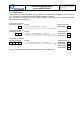
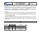
base address
2
register name register mnemonic
9010 0000h Hardware configuration register HWCFG
9011 0000h FPGA control register FCR
9012 0000h LED control register LED
9013 0000h Module control register MCR
9014 0000h I
2
C bus control register I2C
9015 0000h External flag register XF
9016 0000h Watchdog register WDG
9017 0000h PLD version register VER
Table 6: PLD and UART registers of the C6713CPU
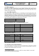
3.10 Description of the PLD Registers
The PLD registers are all 8 bit wide and can be accessed as 8 or 16 bits. All writeable bits can be
read back, so they can be modified without keeping a (shadow register) copy in memory. Bits 0 .. 3
of all PLD registers are reserved. The read-back value of these reserved bits is not defined.
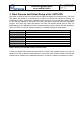
Name Address Bit 7 Bit 6 Bit 5 Bit 4
HWCFG 90100000 RAMSIZE CPUSPEED RESERVED FLASH_A19
FCR 90110000 PROG DONE CFG_EN RESERVED
LED 90120000 LED_RED LED_GREEN
MCR 90130000 SW_RESET RESERVED CTS_RESET_EN RS232_DRV_EN
I2C 90140000 SDA_STAT SDA_CTL SCL_STAT SCL_CTL
XF 90150000 XF1_DIR XF1_DATA XF0_DIR XF0 DATA
WDG 90160000 RESERVED RESERVED WDG_RST WDG_EN
VER 90170000 VERSION
Table 7: PLD register quick reference
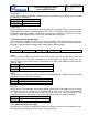
3.10.1 Hardware Configuration Register (HWCFG)
This register provides information about several hardware settings of the board and the controls
the highest address bit of the flash memory. Application software can read this register to
determine e.g. the size of the SDRAM. The value of RAMSIZE and CPUSPEED are determined by
the hardware configuration of the C6713CPU. Please refer to chapter 7.2 for configuration details.
7 6 5 4 3 0
RAMSIZE CPUSPEED RESERVED FLASH_A19 RESERVED
r, 0 r, 0 r, 0 r, w, 0
RAMSIZE:
This bit can be used by application software to determine the available memory
size.
RAMSIZE SDRAM size
0 32 MB
1 64 MB
2
all PLD registers are mirrored within a range of 64K bytes