
Datasheet

17© KEMET Electronics Corporation • KEMET Tower • One East Broward Boulevard C1006_X5R_SMD • 11/9/2018
Fort Lauderdale, FL 33301 USA • 954-766-2800 • www.kemet.com
Surface Mount Multilayer Ceramic Chip Capacitors (SMD MLCCs)
X5R Dielectric, 4 – 50 VDC (Commercial Grade)
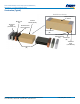
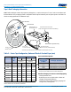
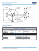
Figure 2 – Punched (Paper) Carrier Tape Dimensions
User Direction of Unreeling
Top Cover Tape
T
Center Lines of Cavity
P
1
ØDo
Po
E
1
F
E
2
W
G
A
0
B
0
Cavity Size,
See
Note 1, Table 7
Bottom Cover Tape
T
1
T
1
Bottom Cover Tape
(10 pitches cumulative
tolerance on tape ±0.2 mm)
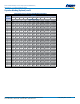
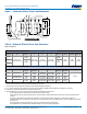
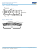
Table 7 – Punched (Paper) Carrier Tape Dimensions
Metricwillgovern
Constant Dimensions — Millimeters (Inches)
Tape Size D
0
E
1
P
0
P
2
T
1
Maximum GMinimum
R Reference
Note 2
8 mm
1.5+0.10-0.0
(0.059+0.004-0.0)
1.75 ±0.10
(0.069 ±0.004)
4.0 ±0.10
(0.157 ±0.004)
2.0 ±0.05
(0.079 ±0.002)
0.10
(0.004)
maximum
0.75
(0.030)
25
(0.984)
Variable Dimensions — Millimeters (Inches)
Tape Size Pitch E2 Minimum F P
1
T Maximum W Maximum A
0
B
0
8 mm Half (2 mm)
6.25
(0.246)
3.5 ±0.05
(0.138 ±0.002)
2.0 ±0.05
(0.079 ±0.002)
1.1
(0.098)
8.3
(0.327)
Note 1
8 mm Single(4mm)
4.0 ±0.10
(0.157 ±0.004)
8.3
(0.327)
1. The cavity de ned by A
0
, B
0
and T shall surround the component with suffi cient clearance that:
a) the component does not protrude beyond either surface of the carrier tape.
b) the component can be removed from the cavity in a vertical direction without mechanical restriction, after the top cover tape has been
removed.
c) rotation of the component is limited to 20° maximum (see Figure 3.)
d) lateral movement of the component is restricted to 0.5 mm maximum (see Figure 4.)
e) see addendum in EIA Standard 481 for standards relating to more precise taping requirements.
2. The tape with or without components shall pass around R without damage (see Figure 6.)