
Datasheet


© KEMET Electronics Corporation • P.O. Box 5928 • Greenville, SC 29606 (864) 963-6300 • www.kemet.com C1016_C0G_ARRAY_SMD • 2/29/2016 88
Surface Mount Multilayer Ceramic Chip Capacitors (SMD MLCCs)
Capacitor Array, C0G Dielectric, 10 – 200 VDC, (Commercial & Automotive Grade)
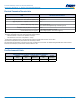
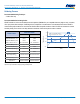
Table 3 – Chip Capacitor Array Land Pattern Design Recommendations per IPC-7351
EIA SIZE
CODE
METRIC
SIZE
CODE
Density Level A:
Maximum (Most) Land
Protrusion (mm)
Density Level B:
Median (Nominal) Land
Protrusion (mm)
Density Level C:
Minimum (Least) Land
Protrusion (mm)
C
Y
X
P
V1
V2
C
Y
X
P
V1
V2
C
Y
X
P
V1
V2
0508/CA052 1220 1.60 1.00 0.55 1.00 3.50 3.30 1.50 0.90 0.50 1.00 2.90 2.80 1.40 0.75 0.45 1.00 2.40 2.50
0612/CA064 1632 1.80 1.10 0.50 0.80 3.90 4.40 1.80 0.95 0.50 0.80 3.30 3.90 1.70 0.85 0.40 0.80 2.80 3.60
Density Level A: For low-density product applications. Provides a wider process window for reow solder processes.
Density Level B: For products with a moderate level of component density. Provides a robust solder attachment condition for reow solder processes.
Density Level C: For high component density product applications. Before adapting the minimum land pattern variations the user should perform qualication
testing based on the conditions outlined in IPC Standard 7351 (IPC–7351).
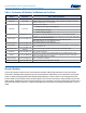
Image below based on Density Level B for an EIA 0612 case size.
Y
V2
V1
Grid Placement Courtyard
X
C
P