
Datasheet


7© KEMET Electronics Corporation • KEMET Tower • One East Broward Boulevard C1017_X7R_ARRAY_SMD • 12/5/2018
Fort Lauderdale, FL 33301 USA • 954-766-2800 • www.kemet.com
7
Surface Mount Multilayer Ceramic Chip Capacitors (SMD MLCCs)
Capacitor Array, X7R Dielectric, 10 – 200 VDC (Commercial & Automotive Grade)
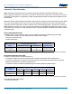
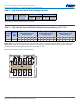
Table 2 – Chip Thickness/Tape & Reel Packaging Quantities
Thickness
Code
Case
Size
Thickness ±
Range (mm)
Paper Quantity Plastic Quantity
7" Reel 13" Reel 7" Reel 13" Reel
MA
0612
0.80 ±0.10
4,000
10,000
0
0
Package quantity based on nished chip thickness specications.
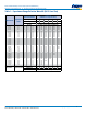
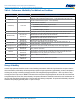
Table 3 – Chip Capacitor Array Land Pattern Design Recommendations per IPC–7351
EIA SIZE
CODE
METRIC
SIZE
CODE
Density Level A:
Maximum (Most) Land
Protrusion (mm)
Density Level B:
Median (Nominal) Land
Protrusion (mm)
Density Level C:
Minimum (Least) Land
Protrusion (mm)
C Y X P V1 V2 C Y X P V1 V2 C Y X P V1 V2
0612/CA064 1632 1.80 1.10 0.50 0.80 3.90 4.40 1.80 0.95 0.50 0.80 3.30 3.90 1.70 0.85 0.40 0.80 2.80 3.60
Density Level A: For low-density product applications. Provides a wider process window for reow solder processes.
Density Level B: For products with a moderate level of component density. Provides a robust solder attachment condition for reow solder processes.
Density Level C: For high component density product applications. Before adapting the minimum land pattern variations, the user should perform
qualication testing based on the conditions outlined in IPC Standard 7351 (IPC–7351).
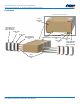
Image below based on Density Level B for an EIA 0612 case size.
Y
V2
V1
Grid Placement Courtyard
X
C
P