
Datasheet


15© KEMET Electronics Corporation • KEMET Tower • One East Broward Boulevard T2005_T491 • 3/11/2019
Fort Lauderdale, FL 33301 USA • 954-766-2800 • www.kemet.com
15
Tantalum Surface Mount Capacitors – Standard Tantalum
T491 Industrial Grade MnO
2
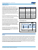
Reverse Voltage
Solid tantalum capacitors are polar devices and may be permanently damaged or destroyed if connected with the wrong
polarity.Thepositiveterminalisidentiedonthecapacitorbodybyastripe,plus,insomecasesabevelededge.Asmall
degree of transient reverse voltage is permissible for short periods per the table. The capacitors should not be operated
continuously in reverse mode, even within these limits.
Temperature Permissible Transient Reverse Voltage
25°C
15% of Rated Voltage
85°C
5% of Rated Voltage
125°C
1% of Rated Voltage
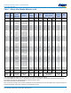
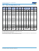
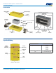
Table 2 – Land Dimensions/Courtyard
KEMET
Metric
Size
Code
Density Level A:
Maximum (Most) Land
Protrusion (mm)
Density Level B:
Median (Nominal) Land
Protrusion (mm)
Density Level C:
Minimum (Least) Land
Protrusion (mm)
Case EIA W L S V1 V2 W L S V1 V2 W L S V1 V2
A 3216–18 1.35 2.20 0.62 6.02 2.80 1.23 1.80 0.82 4.92 2.30 1.13 1.42 0.98 4.06 2.04
B 3528–21 2.35 2.21 0.92 6.32 4.00 2.23 1.80 1.12 5.22 3.50 2.13 1.42 1.28 4.36 3.24
C
6032–28
2.35
2.77
2.37
8.92
4.50
2.23
2.37
2.57
7.82
4.00
2.13
1.99
2.73
6.96
3.74
D 7343–31 2.55 2.77 3.67 10.22 5.60 2.43 2.37 3.87 9.12 5.10 2.33 1.99 4.03 8.26 4.84
E
1
7360–38 3.25 2.77 3.67 10.22 7.30 3.13 2.37 3.87 9.12 6.80 3.03 1.99 4.03 8.26 6.54
M 3528-15 2.35 2.20 0.92 6.32 4.00 2.23 1.80 1.12 5.22 3.50 2.13 1.42 1.28 4.36 3.24
S
2
3216–12 1.35 2.20 0.62 6.02 2.80 1.23 1.80 0.82 4.92 2.30 1.13 1.42 0.98 4.06 2.04
T
3528–12
2.35
2.20
0.92
6.32
4.00
2.23
1.80
1.12
5.22
3.50
2.13
1.42
1.28
4.36
3.24
U 6032–15 2.35 2.77 2.37 8.92 4.50 2.23 2.37 2.57 7.82 4.00 2.13 1.99 2.73 6.96 3.74
V 7343–21 2.55 2.77 3.67 10.22 5.60 2.43 2.37 3.87 9.12 5.10 2.33 1.99 4.03 8.26 4.84
W 7343–15 2.55 2.77 3.67 10.22 5.60 2.43 2.37 3.87 9.12 5.10 2.33 1.99 4.03 8.26 4.84
X
1
7343–43 2.55 2.77 3.67 10.22 5.60 2.43 2.37 3.87 9.12 5.10 2.33 1.99 4.03 8.26 4.84
Density Level A: For low-density product applications. Recommended for wave solder applications and provides a wider process window for reow
solder processes.
Density Level B: For products with a moderate level of component density. Provides a robust solder attachment condition for reow solder processes.
Density Level C: For high component density product applications. Before adapting the minimum land pattern variations, the user should perform
qualication testing based on the conditions outlined in IPC standard 7351 (IPC–7351).
1
Height of these chips may create problems in wave soldering.
2
Land pattern geometry is too small for silkscreen outline.
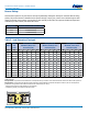
L
S
W W
L
V1
V2
Grid Placement Courtyard