PCI-1712/1712L User's manual 1 MS/s, 12-bit, 16-ch HighSpeed Multifunction Card
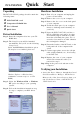
PCI-1712/1712L Quick Start Unpacking Hardware Installation The PCI-1712/1712L package should contain the following items: Step 1: Turn off your computer and unplug the power cord and cables þ þ þ þ Step 2: Remove the cover of your computer PCI-1712/1712L card Companion CD-ROM disc User’s Manual Quick Start Driver Installation Step 1: Insert the companion disc into your CDROM drive. Step 2: The Setup Program will be launched automatically, and you’ll see the following Setup Screen.
Device Installation Step 1: Run the Device Installation program (by accessing Start/Programs/ Advantech Driver for 95 and 98 (or for NT)/Device Installation). Step 2: On the Device Installation program window, select the Device menu item on the menu bar, and click the Setup command to bring up the I/O Device Installation dialog box as below: Step 6: After your card is properly installed and configured, you can click the Test button to test your hardware.
Copyright® This documentation and the software included with this product are copyrighted 2001 by Advantech Co., Ltd. All rights are reserved. Advantech Co., Ltd. reserves the right to make improvements in the products described in this manual at any time without notice. No part of this manual may be reproduced, copied, translated or transmitted in any form or by any means without the prior written permission of Advantech Co., Ltd.
Contents 1. Introduction ................................................................. 1 1.1 1.2 1.3 Features ......................................................................................... 1 Installation Guide ........................................................................... 3 Accessories ................................................................................... 5 2. Installation .................................................................. 7 2.1 2.2 2.3 2.4 2.
. Calibration ................................................................. 55 6.1 VR Assignment ............................................................................... 55 6.2 A/D Calibration ............................................................................... 56 6.3 D/A Calibration ............................................................................... 57 6.4 Calibration Utility ............................................................................ 58 Appendix A.
D.14 Counter gate and clock control/status — Write/ Read BASE+20 to 26 ............................................................................................. 96 D.15 Digital I/O registers — Write/Read BASE+28 .............................. 99 D.16 Digital I/O configuration registers — Write/Read BASE+2A .... 100 D.17 Calibration command registers — Write BASE+2C ................... 100 D.18 D/A Channel Data for Continuous Output Operation Mode — Write BASE+30 .........................................
Figures Figure 2-1: The Setup Screen of Advantech Automation Software ....... 8 Figure 2-2: Different options for Driver Setup ....................................... 9 Figure 2-3: The device name listed on the Device Manager ............... 11 Figure 2-4: The Advantech Device Installation utility program ............ 12 Figure 2-5: The I/O Device Installation dialog box .............................. 12 Figure 2-6: The Device(s) Found dialog box ....................................
Figure 6-4: Auto A/D Calibration Dialog Box ..................................... 59 Figure 6-5: A/D Calibration Procedure 1 ............................................ 60 Figure 6-6: A/D Calibration Procedure 2 ............................................ 60 Figure 6-7: A/D Calibration Procedure 3 ............................................ 61 Figure 6-8: A/D Calibration is finished ............................................... 61 Figure 6-9: Range Selection in D/A Calibration .........................
Tables Table 3-1: Table 3-1: Table 3-1: Table 5-1: Table 5-2: Table 5-3: I/O Connector Signal Description (Part 1) ........................ 21 I/O Connector Signal Description (Part 2) ........................ 22 I/O Connector Signal Description (Part 3) ........................ 23 Gains and Analog Input Range ........................................ 33 Analog Input Data Format ............................................... 39 The corresponding Full Scale values for various Input Voltage Ranges ..........
Table D-19: Table D-20: Table D-21: Table D-22: Table D-23: Table D-24: Register for Digital I/O ..................................................... 99 Register for digital I/O configuration ............................... 100 Register for digital I/O configuration ............................... 100 Register for calibration command .................................. 100 Calibration command .................................................... 101 Register for D/A channel data ............................
1 Chapter 1 Chapter 1. Introduction Thank you for buying the Advantech PCI-1712/1712L PCI card. The PCI-1712/1712L is a powerful high-speed multifunction DAS card for PCI bus. It features a 1MHz 12-bit A/D converter, an on-board FIFO buffer (storing up to 1K samples for A/D, and up to 32K samples for D/ A conversion).
Chapter 1 PCI-Bus Mastering Data Transfer The PCI-1712/1712L supports PCI-Bus mastering DMA for high-speed data transfer and gap-free analog input and analog output. By setting aside a block of memory in the PC, the PCI-1712/1712L performs busmastering data transfers without CPU intervention, setting the CPU free to perform other more urgent tasks such as data analysis and graphic manipulation. The function allows users to run all I/O functions simultaneously at full speed without losing data.
Chapter 1 Continuous Analog Output The PCI-1712 provides two analog output channels. Both of them can perform continuous waveform output. The analog output can be up to 500kS/s for each analog output channel. Or you can load a cyclic waveform into an on-board FIFO, which will continuously output the cyclic waveform. The on-board FIFO of the PCI-1712 can store 2 to 32K samples for the waveform output.
Chapter 1 Figure 1-1: Installation Flow Chart PCI-1712/1712L User’s Manual –4– Advantech Co., Ltd. www.advantech.
Chapter 1 q Application software ActiveDAQ, GeniDAQ or other third-party software packages After you have got the necessary components and maybe some accessories for enhanced operation of your DAS card, you can then begin the Installation procedures. Figure 1-1 on the next page provides a concise flow chart to give users a broad picture of the software and hardware installation procedures: 1.3 Accessories Advantech offers a complete set of accessory products to support the PCI-1712/1712L cards.
Chapter 1 l Industrial-grade screw-clamp terminal blocks for heavy-duty and reliable connections. PCI-1712/1712L User’s Manual –6– Advantech Co., Ltd. www.advantech.
2 Chapter 1 Chapter 2. Installation This chapter gives users a package item checklist, proper instructions about unpacking and step-by-step procedures for both driver and card installation. 2.1 Unpacking After receiving your PCI-1712/1712L package, please inspect its contents first.
Chapter 2 Whenever you handle the card, grasp it only by its edges. DO NOT TOUCH the exposed metal pins of the connector or the electronic components. Note: ✎ Keep the antistatic bag for future use. You might need the original bag to store the card if you have to remove the card from PC or transport it elsewhere. 2.2 Driver Installation We recommend you to install the driver before you install the PCI1712/1712L card into your system, since this will guarantee a smooth installation process.
Chapter 2 Step 3: Select the DLL Drivers option. Step 4: Select the Windows 95/98 or Windows NT option according to your operating system. Just follow the installation instructions step by step to complete your DLL driver setup. Figure 2-2: Different options for Driver Setup For further information on driver-related issues, an online version of DLL Drivers Manual is available by accessing the following path: Start/Programs/Advantech Driver for 95 and 98 (or for NT)/Driver Manual 2.
Chapter 2 Step 2: Remove the cover of your computer. Step 3: Remove the slot cover on the back panel of your computer. Step 4: Touch the metal part on the surface of your computer to neutralize the static electricity that might be on your body. Step 5: Insert the PCI-1712/1712L card into a PCI slot. Hold the card only by its edges and carefully align it with the slot. Insert the card firmly into place. Use of excessive force must be avoided, otherwise the card might be damaged.
Chapter 2 Figure 2-3: The device name listed on the Device Manager Note: ✎ If your card is properly installed, you should see the device name of your card listed on the Device Manager tab. If you do see your device name listed on it but marked with an exclamation sign “!” , it means your card has not been correctly installed. In this case, remove the card device from the Device Manager by selecting its device name and press the Remove button. Then go through the driver installation process again.
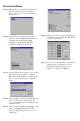
Chapter 2 2.4 Device Setup & Configuration The Device Installation program is a utility that allows you to set up, configure and test your device, and later stores your settings on the system registry. These settings will be used when you call the APIs of Advantech 32-bit DLL drivers. Setting Up the Device Step 1: To install the I/O device for your card, you must first run the Device Installation program (by accessing Start/Programs/ Advantech Driver for 95 and 98 (or for NT)/Device Installation).
Chapter 2 Step 3: Scroll down the List of Devices box to find the device that you wish to install, then click the Add button to evoke the Device(s) Found dialog box such as one shown in Fig. 2-6. The Device(s) Found dialog box lists all the installed devices on your system. Select the device you want to configure from the list box and press the OK button. After you have clicked OK, you will see a Device Setting dialog box such as the one in Fig. 2-7.
Chapter 2 output voltage range. When selecting voltage source as Internal, users will have options for the output voltage ranges : 0 ~ 5V and 0 ~ 10V for unipolar; -5 ~ 5V and -10 ~ 10V for bipolar.
Chapter 2 2.5 Device Testing Following through the Setup and Configuration procedures to the last step described in the previous section, you can now proceed to test the device by clicking the Test Button on the I/O Device Installation dialog box (Fig. 2-8).
Chapter 2 Figure 2-10: Analog Input tab on the Device Test dialog box Testing Analog Output Function (PCI-1712 only) Click the Analog Output tab to bring it up to the foreground. The Analog Output tab allows you to output quasi-sine, triangle, or square waveforms generated by the software automatically, or output single values manually. You can also configure the waveform frequency and output voltage range.
Chapter 2 Figure 2-12: Digital Input tab on the Device Test dialog box Testing Digital Output Function Click the Digital Output tab to bring up the Digital Output test panel such as seen on the next page. By pressing the buttons on each tab, users can easily set each digital output channel as high or low for the corresponding port. Figure 2-13: Digital Output tab on the Device Test dialog box Testing Counter Function Click the Counter Tab to bring its test panel forth.
Chapter 2 configure the Pulse Frequency by the scroll bar right below it. Figure 2-14: Digital output tab on the Device Test dialog box Only after your card device is properly set up, configured and tested, can the device installation procedure be counted as complete. After the device installation procedure is completed, you can now safely proceed to the next chpater, Signal Connections. PCI-1712/1712L User’s Manual – 18 – Advantech Co., Ltd. www.advantech.
3 Chapter 3 3. Signal Connections Chapter 3.1 Overview Maintaining proper signal connections is one of the most important factors to ensure that your application system is sending and receiving data correctly. A good signal connection can avoid unnecessary and costly damage to your PC and other hardware devices. This chapter provides useful information about how to connect input and output signals to the PCI-1712/1712L via the I/O connector. 3.
Chapter 3 Figure 3-1: I/O connector pin assignments for the PCI-1712/1712L *: Pins 20, 22~25, 54, 56~59 are not defined on PCI-1712L PCI-1712/1712L User’s Manual – 20 – Advantech Co., Ltd. www.advantech.
Chapter 3 I/O Connector Signal Description Signal Name Reference Direction Description AI<0...15> AIGND Input Analog Input Channels 0 through 15. Each channel pair, AI (i = 0...7), can be configured as either one differential input or two single-ended inputs. AIGND - - Analog Input Ground. These pins are the reference points for single-ended measurements and the bias current return point for differential measurement.
Chapter 3 Signal Name Reference Direction Description DIO<0..15> DGND Input Digital Input / Output signals. These pins are digital input / output channel 0 to 15 AI_CLK DGND Input Analog Input external clock input. This is the external clock input for the analog input. AI_TRG DGND Input Analog Input TTL Trigger- This is the TTL trigger for analog trigger. AI_CLK_OUT DGND Output Analog Input Clock Output. This pin pulses once for each pacer clock.
Chapter 3 Signal Name Reference Direction Description CNT0_CLK DGND Input Counter 0 Clock Input. This pin is the counter 0 external clock input (up to 10MHz), counter 0 clock can be either internal set by software. CNT0_GATE DGND Input Counter 0 Gate Input. This pin is for counter 0 gate control, see 82C54 data sheet for detailed information. CNT0_OUT DGND Output Counter 0 Output. This pin is counter 0 output, see 82C54 data sheet for detailed information.
Chapter 3 3.3 Analog Input Connections The PCI-1712/1712L supports either 16 single-ended or 8 differential analog inputs. Each individual input channel is software-selected. Single-ended Channel Connections The single-ended input configuration has only one signal wire for each channel, and the measured voltage (Vm) is the voltage of the wire as referenced against the common ground. A signal source without a local ground is also called a “floating source”.
Chapter 3 same voltage. The difference between the ground voltages forms a common-mode voltage (Vcm). To avoid the ground loop noise effect caused by common-mode voltages, you can connect the signal ground to the Low input. Figure 3-3 shows a differential channel connection between a groundreference signal source and an input channel on the PCI-1712/1712L. With this connection, the PGIA rejects a common-mode voltage Vcm between the signal source and the PCI-1712/1712L ground, shown as Vcm in Figure 3-3.
Chapter 3 Figure 3-4: Differential input channel connection - floating signal source However, this connection has the disadvantage of loading the source down with the series combination (sum) of the two resistors. For ra and rb, for example, if the input impedance rs is 1 kΩ, and each of the two resistors is 100 kW, then the resistors load down the signal source with 200 kΩ (100 kΩ + 100 kΩ), resulting in a –0.5% gain error.
Chapter 3 3.4 Analog Output Connections The PCI-1712 provides two D/A output channels, AO0_OUT and AO1_OUT. Users may use the PCI-1712 internally-provided precision +5V (+10V) reference to generate 0 ~ +5 V and 0 ~ +10 V unipolar D/A output range; or to generate -5 ~ +5 V and -10 ~ +10 V for bipolar output range. Users may also set D/A output range through external references, AO0_REF and AO1_REF. The external reference input range is 0~10 V.
Chapter 3 3.5 Field Wiring Considerations When you use the PCI-1712/1712L to acquire data from outside, noises in the environment might significantly affect the accuracy of your measurements if due cautions are not taken. The following measures will be helpful to reduce possible interference running signal wires between signal sources and the PCI-1712/1712L.
4 Chapter 4 4. Software Overview Chapter This chapter gives you an overview of the software programming choices available and a quick reference to source codes examples that can help you be better oriented to programming. After following the instructions given in Chapter 2, it is hoped that you feel comfortable enough to proceed further. Programming choices for DAS cards: You may use Advantech application software such as Advantech DLL driver.
Chapter 4 4.2 DLL Driver Programming Roadmap This section will provide you a roadmap to demonstrate how to build an application from scratch using Advantech DLL driver with your favorite development tools such as Visual C++, Visual Basic, Delphi and C++ Builder. The step-by-step instructions on how to build your own applications using each development tool will be given in the DLL Drivers Manual. Moreover, a rich set of example source codes are also given for your reference.
Chapter 4 Programming with DLL Driver Function Library Advanech DLL driver offers a rich function library to be utilized in various application programs. This function library consists of numerous APIs that support many development tools, such as Visual C++, Visual Basic, Delphi and C++ Builder.
Chapter 4 PCI-1712/1712L User’s Manual – 32 – Advantech Co., Ltd. www.advantech.
5 Chapter 4 5. Principles of Operation Chapter This chapter describes the analog input, analog output, digital I/O and counter/timer features of the PCI-1712/1712L card. 5.
Chapter 5 Analog Input Acquisition Modes The PCI-1712/1712L can acquire data in single value, pacer, posttrigger, delay-trigger, about-trigger and pre-trigger acquisition modes. These analog input acquisition modes are described in more detail in the followings: q Single Value Acquisition Mode The single value acquisition mode is the simplest way to acquire data. Once the software issues a trigger command, the A/D converter will convert one data, and return it immediately.
Chapter 5 Trigger Event Acquired number of samples N 1st 2nd 3rd N-2th N-1th Nth t Figure 5-1: Post-Trigger Acquisition Mode q Delay Trigger Acquisition Mode In delay trigger mode, data acquisition will be activated after a preset delay number of sample has been taken after the trigger event. The delay number of sample ranges from 2 to 65535 as defined in DMA counter.
Chapter 5 w w w w w Set to About-Trigger Acquisition Mode The sample clock source and sample rate The trigger source and edge type The total acquired sample number N The specific sample number M before the trigger event. The range of preset sample number is 2 samples minimum and is limited on basis of memory size of your host PC. In about-trigger mode, users must first designate the size of the allocated memory and the amount of samples to be snatched after the trigger event happens.
Chapter 5 Trigger Event Acquired number of samples N 1 2 2 Samples N 3 N+1 N+2 t Figure 5-4: Pre-Trigger Acquisition Mode A/D Sample Clock Sources The PCI-1712/1712L can adopt both internal and external clock sources for pacer, post-trigger, delay-trigger, about-trigger acquisition modes: w Internal A/D sample clock with 16-bit Counter w External A/D sample clock that is connected to AI_CLK on the PCLD-8712 screw terminal board.
Chapter 5 Figure 5-5: PCI-1712/1712L Sample Clock Source Trigger Sources The PCI-1712/1712L supports the following trigger sources for post-, delay-, about- and pre-trigger acquisition modes: w Software trigger, w External digital (TTL) trigger, and w Analog threshold trigger. With PCI-1712/1712L, user can define the type of trigger source as rising-edge or falling-edge. These following sections describe these trigger sources in more detail.
Chapter 5 the PCLD-8712 screw terminal board. The trigger signal is TTLcompatible. q Analog Threshold Trigger For analog input operations, an analog trigger event occurs when the PCI-1712/1712L detects a transition from above a threshold level to below a threshold level (falling edge), or a transition from below a threshold level to above a threshold level (rising edge).
Chapter 5 5.2 Analog Output Features The PCI-1712 card provides two 12-bit multi-range analog output (D/A) channels. This section describes the following features of the D/A functions: w Analog output ranges w Analog output operation modes w D/A output clock sources w Trigger sources w Analog Output Data Format Analog Output Ranges The PCI-1712 provides two 12-bit analog output channels, both of which can be configured to be applicable within 0 ~ 5 V, 0 ~ 10 V, ± 5 V, ± 10 V output voltage range.
Chapter 5 channel. In this mode, users need to set the clock source and trigger source first, and then generate the output data to be stored in the memory buffers of host PC. The host computer then transfers those data to be written to the DACs from its buffers to the 32K-sample Output FIFO on board. When it detects a trigger, the board outputs the values in the Output FIFO to the DACs at the same time. When the samples in FIFO decreases to less than half size (i.e.
Chapter 5 the analog output operation. The minimum frequency is 156.2 S/s, the maximum frequency is 1 MS/s. q External D/A Output Clock The external D/A output clock is useful when you want to pace analog output operations at rates not available with the internal D/A output clock, or when you want to pace at uneven intervals, or when you want to start pacing on an external trigger event. Connect an external D/A output clock to screw terminal AO_CLK on the PCLD-8712 screw terminal board.
Chapter 5 Analog Output Data Format Table 5-4: Analog Output Data Format D/A code Mapping Voltage Hex. Dec. Unipolar Bipolar 000h 0d 0 -FS/2 7FFh 2047d FS/2 - 1 LSB -1 LSB 800h 2048d FS/2 0 FFFh 4095d FS - 1 LSB FS/2 - 1 LSB FS/4096 FS/4096 1 LSB Table 5-5: The corresponding Full Scale values for various Output Voltage Ranges Reference Source Internal External Uniplar Range Bipolar FS Range FS 0~5V 5 ±5V 10 0 ~ 10 V 10 ± 10 V 20 0~xV x ±xV 2x 5.
Chapter 5 5.4 Counter/Timer Features The PCI-1712/1712L features multifunction counter/timer functions with one-shot, rate generation, frequency measurement and pulse width measurement. There are two 8254 counter chips in PCI-1712/ 1712L, and each chip has 3 multifunction counters. The first counter chip (chip 1) is specified for AI and AO functions, and can’t be used by user. The second counter chip (chip 2) is reserved for user, and the following section describes its features.
Chapter 5 0, 1 and 2. You can choose any counter to be your first cascaded counter, and the next counter would the next one in the round-robin order. For example, if you would like to cascade two 16-bit counters into one 32-bit counter, and you choose counter 1 to be the first counter then the next counter you choose should be counter 2. Gate Types and Sources The gate types and sources you select determine what kind of gate input signal to enable your counter/timer when receiving clock input.
Chapter 5 Counter/timer operation modes We enhance the gate function for more applications. For example, event counting, rate generation, one shot, frequency measurement and pulse width measurement. We make some innovative arrangements of clock and gate of counter. For detailed information, please refer to Appendix D.12 to D.14 and Intel® 82C54 User’s Manual. The following sections show how to implement counter functions.
Chapter 5 appropriate depending on your application. Please follow the procedure below when using software: 1 Select a counter (e.g. counter 0) to do rate generation. 2. Set the counter in mode 3 (Please refer to Intel® 82C54 User’s Manual). 3. Select the clock input of the counter. (Could be internal or external) 4. Set the gate type of the counter to positive (logic-high). 5. Set the value of the counter to serve as the factor with which to divide the clock input frequency. 6.
Chapter 5 q Frequency measurement The frequency measurement function helps user to measure the frequency of the signal from counter-associated clock input on PCLD8712. Frequency measurement needs two counters to implement. Use the first counter to produce a one-shot pulse with defined pulse period to be the second counter’s gate. Connect the signal source, whose frequency is to be measured, to the clock input of the second counter.
Chapter 5 Figure 5-6: Frequency measurement The following C program serves as an example to explain how to implement the frequency measurement by software. outport(addr2_1712+0x26,0x03); while(!kbhit()) { //Initialize CNT1 and CNT2 outport(addr2_1712+0x24,0x00); outport(addr2_1712+0x22,0x00); // Set internal clock as 10 KHz //Setup CNT1 to output 1 sec.
Chapter 5 //Set the value of CRT2 as 65,535 for down counting outport(addr2_1712+0x24,0x80); //Set CNT2’s gate input as high outport(addr2_1712+0x24,0x88); outport(addr2_1712+0x24,0x00); /*Generate one clock to CNT2, and set CNT2’s gate input as low*/ outport(addr2_1712+0x24,0x52); /*Set CNT2’s clock source as external from CNT1’s OUT, and negative polarity*/ outport(addr2_1712+0x22,0x80); outport(addr2_1712+0x22,0x88); outport(addr2_1712+0x22,0x80); outport(addr2_1712+0x22,0x81); //Set CNT1’s gate input a
Chapter 5 printf(“Counter 2 = %u \n”,old_count); old_count = 0; } q Pulse width measurement The pulse width measurement function helps user measure the period of the signal from counter-associated clock input on PCLD-8712. Pulse width measurement also needs two counters to implement. Use the first counter to measure the positive period of the pulse and second counter to measure the negative period of the pulse (In DLL driver, it uses CNT1 and CNT2 to implement the pulse width measurement function).
Chapter 5 (65535-50000)/1K = 15.535 sec. Figure 5-7: Pulse width measurement The following C program is the example to explain how to implement the pulse width measurement by software.
Chapter 5 internal, and gate use for pulse width measurement*/ outport(addr2_1712+0x22,0x80); outport(addr2_1712+0x22,0x88); outport(addr2_1712+0x22,0x71); //Set CNT1’s gate input as high //Generate one clock to CNT1 /*Set CNT1’s clock source as internal, gate use for pulse width measurement, and negative polarity*/ /*Reset pulse width measurement state machine, and check if CNT2’s gate input receives the measured signal*/ while(1) { outport(addr2_1712+0x24,0x0031); //Generate a rising edge to //reset the
Chapter 5 //CNT1’s gate input received the measured signal, check if finished? while(1) { i = inport(addr2_1712+0x22) & 0x0800; if(i == 0x0000) break; //CNT1’s gate input is low } /*The CNT1 & 2 has finished the job, and then show the measured period on display*/ dl= inport(addr2_1712+0x1a); //Read low byte dh= inport(addr2_1712+0x1a)<<8; //Read high byte dh= dh + (dl & 0x00ff); neg_count = 0xffff - dh ; dl= inport(addr2_1712+0x1c); dh= inport(addr2_1712+0x1c)<<8; dh= dh + (dl & 0x00ff); pos_count = 0xffff
6 Chapter 6 Chapter 6. Calibration This chapter provides brief information on PCI-1712/1712L calibration. Regular calibration checks are important to maintain accuracy in data acquisition and control applications. A calibration utility, AutoCali, is included on the companion CD-ROM : AutoCali.EXE PCI-1712/1712L calibration utility This calibration utility is designed for the Microsoft©Windows™ environment.
Chapter 6 6.2 A/D Calibration Regular and proper calibration procedures ensure the maximum possible accuracy. It is easy to complete the A/D calibration procedure automatically (i.e. through software calibration) by executing the A/D calibration program AutoCali. Therefore, it is not necessary to adjust the hardware settings of the PCI-1712/1712L. However, the following calibration steps are also provided for your reference in case manual calibration is needed: 1.
Chapter 6 mode. Adjust the gain until the AI0’s value converges between 0 and 1. 7. Repeat steps 4 to 6 several times. 6.3 D/A Calibration You can select an on-board +5V or +10V internal reference voltage or an external voltage as your analog output reference voltage. If you use an external reference, connect the reference voltage within the ±10V range to the reference input of the D/A output channel you want to calibrate.
Chapter 6 the AOn output code reads AI4+2n equals 0x0001. 8. Set the bipolar output range of AO0 and AO1 the same as the reference voltage within -10 to +10 V. 9. Set the output value of AOn data register (BASE+0x0C) as 0x0800 and output to AOn. 10.Adjust teh associated bipolar offset register (BASE+0x2C) until the AOn output code reads AI4+2n equals 0x0800. 11.Repeat steps 3 to 10 several times. 6.
Chapter 6 Step 3: After you start to calibrate the PCI-1712/1712L, please don’t forget to adjust VR1. Figure 6-3: Warning message before start calibration A/D channel Auto-Calibration Step 4: Click the Auto A/D Calibration tab to show the A/D channel auto-calibration panel (Fig. 6-4). Press the start button to calibrate A/D channels automatically. Figure 6-4: Auto A/D Calibration Dialog Box Advantech Co., Ltd. www.advantech.
Chapter 6 Step 5: The first A/D calibration procedure is enabled (Fig. 6-5). Figure 6-5: A/D Calibration Procedure 1 Step 6: The second A/D calibration procedure is enabled (Fig. 6-6) Figure 6-6: A/D Calibration Procedure 2 PCI-1712/1712L User’s Manual – 60 – Advantech Co., Ltd. www.advantech.
Chapter 6 Step 7: The third A/D calibration procedure is enabled (Fig. 6-7) Figure 6-7: A/D Calibration Procedure 3 Step 8: Auto-calibration is finished. (See fig. 6-8) Figure 6-8: A/D Calibration is finished Advantech Co., Ltd. www.advantech.
Chapter 6 D/A channel Auto-Calibration Step 9: Click the Auto D/A Calibration tab to show the D/A channel auto calibration panel. Please finish the A/D calibration procedure first before you start the D/A calibration procedure. There are two D/A channels in PCI-1712; select the output range for each channel and then press the start button to calibrate D/A channels (Fig. 6-9). Figure 6-9: Range Selection in D/A Calibration Step 10: D/A channel 0 calibration is enabled (Fig.
Chapter 6 Step 11: D/A channel 1 calibration is enabled (Fig. 6-11) Figure 6-11: Calibrating D/A Channel 1 Step 12: Auto-calibration is finished (Fig. 6-12) Figure 6-12: D/A Calibration is finished Advantech Co., Ltd. www.advantech.
Chapter 6 A/D channel Manual-Calibration Step 1: Click the Manual A/D Calibration tab to show the A/D channel manual calibration panel. Before calibrating, acquire the reference voltage from a precision standard voltage reference. Go to the Range form, select a channel and the target voltage range according to the input voltage value from a precision standard voltage reference(Fig. 6-13).
Chapter 6 Step 2: According to the difference between reference voltage and receiving data in PCI-1712/1712L, adjust the gain, bipolar offset and unipolar offset registers (Figure 6-14) Figure 6-14: Adjusting registers Step 3: Adjust the registers until they fall between the input voltage from the standard voltage reference and the receiving voltage reflectected in the Manual A/D Calibration tab. Advantech Co., Ltd. www.advantech.
Chapter 6 D/A channel Manual-Calibration Step 1: Click the Manual D/A Calibration tab to show the D/A channel manual calibration panel. Two D/A channels are individually calibrated . Before calibrating, output desired voltage from the D/A channels and measure it through an external precision multimeter. Step 2: For example, choose channel 0; select the Range and select the wished output voltage code or value from the radio buttons (Fig. 6-15 and Fig. 6-16).
Chapter 6 Step 3: According to the difference between the output voltage from D/A channel and the value in the multimeter, adjust the gain, bipolar offset and unipolar offset registers (Fig. 6-17) Figure 6-17: Adjusting registers Step 4: Adjust registers until they fall between the output voltage from the D/A channel and the value in the multimeter. Advantech Co., Ltd. www.advantech.
Chapter 6 PCI-1712/1712L User’s Manual – 68 – Advantech Co., Ltd. www.advantech.
A Chapter 4 Appendix A. Specification Analog Input: Channels 16 single-ended or 8 differential or combination Resolution 12-bit FIFO Size 1K samples Max. Transfer Rate Conversion Time Input range and Gain List Drift Small Signal Bandwidth for PGA Common mode voltage Max. Input voltage Input Protect Input Impedance Trigger Mode Multi-channel, single gain: 1 MS/s Multi-channel, multi-gain: 600 kS/s Multi-channel, multi-gain, unipolar/bipolar: 400 kS/s 500 ns Gain 0.
APPENDIX A Analog Output: (PCI-1712 only) Channels 2 Resolution 12-bit FIFO Size 32K samples Operation mode Output Range (Internal & External Reference) Accuracy Single output, continuous output, waveform output Using Internal Reference 0~+5V,0~+10 V, -5~+5V,-10~+10V Using External Reference 0 ~ +x V@ +x V (-10 ≤ x ≤ 10 -x ~ +x V@ +x V (-10 ≤ x ≤ 10) Relative ± 1 LSB Differential Non-linearity ± 1 LSB (monotonic) Offset < 1 LSB Slew Rate 20V/µs Drift Driving Capability 10 ppm/° C ± 10mA
APPENDIX A Counter/Timer: Channels Resolution Compatibility Base Clock Max. Input Frequency Clock Input Gate Input Counter Output 3 16-bit TTL level 10 MHz, 1MHz, 100kHz, 10kHz 10 MHz Low 0.8 V max. High 2.0 V min. Low 0.8 V max. High 2.0 V min. Low 0.5 V max.@+24 mA High 2.4 V min.@-15 mA General: I/O Connector Type Dimensions Power Consumption Temperature 68-pin SCSI-II female 175 mm x 100 mm (6.9" x 3.9") Typical +5 V @ 850 mA +12 V @ 600 mA Max.
APPENDIX A PCI-1712/1712L User’s Manual – 72 – Advantech Co., Ltd. www.advantech.
B APPENDIX B Appendix B. Block Diagram Block Diagram PCI BUS 8 b it D /A C L K [3 :0 ] G AT E [3 :0 ] 40MHz OSC.
APPENDIX B PCI-1712/1712L User’s Manual – 74 – Advantech Co., Ltd. www.advantech.
C APPENDIX C C. Screw-terminal Board Appendix C. 1 Introduction The PCLD-8712 Screw-terminal Board provides convenient and reliable signal wiring for the PCI-1712/1712L of which has a 68-pin SCSI-II connector. Due to its special PCB layout you can install passive components to construct your own signal-conditioning circuits. The user can easily construct a low-pass filter, attenuator or current shunt converter by adding resistors and capacitors on board’s circuit pads. C.
APPENDIX C CN1: 68-pin SCSI-II connector for connection with the PCI-1712 CN2: 20-pin connector for digital I/O C.4 Pin Assignment CN2 DIO 0 1 2 DIO 1 DIO 2 3 4 DIO 3 DIO 4 5 6 DIO 5 DIO 6 7 8 DIO 7 DIO 8 9 10 DIO 9 DIO 10 11 12 DIO 11 DIO 12 13 14 DIO 13 DIO 14 15 16 DIO 15 DGND 17 18 DGND +5 V 19 20 +12 V Figure C-2: CN2 pin assignments for the PCLD-8712 PCI-1712/1712L User’s Manual – 76 – Advantech Co., Ltd. www.advantech.
APPENDIX C C.5 Single-ended Connections a) Straight-through connection (factory setting) RAn = 0 Ω (short) RBn = none Cn = none b) 1.6 kHz (3dB) low pass filter RAn = 10 k Ω RBn = none Cn = 0.01 µF 1 f3dB = 2πKRAnCn c) 10 : 1 voltage attenuator: RAn = 9 k Ω RBn = 1 k Ω Cn = none Attenuation = RAnRBn + RBn d) 4 ~ 20 mA to 1 ~ 5 VDC signal converter: RAn = 0 Ω (short) RBn = 250 Ω (0.1% precision resistor) Cn = none Advantech Co., Ltd. www.advantech.
APPENDIX C C.6 Differential Connections a) Straight-through connection (factory setting): RAn = 0 Ω (short) RAn+1 = 0 Ω (short) RDn = none CDn = none b) 1.6 kHz (3dB) low pass filter RAn = 5 kΩ RAn+1 = 5 kΩ RDn = none CDn = 0.01 µF 1 f3dB = 2π (RAn+RAn+1) CDn c) 10 : 1 voltage attenuator: RAn = 4.5 k Ω RAn+1 = 4.5 kΩ RDn = 1 kΩ Cn = none RDn Attenuation = RAn+RAn+1+RDn d) 4 ~ 20 mA to 1 ~ 5 VDC signal converter: RAn = 0 Ω (short) RAn+1 = 0 Ω (short) RDn = 250 Ω (0.1% precision resistor) CDn = none 3.
D APPENDIX D Appendix D. Register Structure and Format D.1 Overview The PCI-1712/1712L is delivered with an easy-to-use 32-bit DLL driver for user programming under Windows 95/98/NT operating system. We dvise users to program the PCI-1712/1712L using 32-bit DLL driver provided by Advantech to avoid the complexity of low-level programming by register. The most important consideration in programming the PCI-1712/1712L at the register level is to understand the function of the card’s registers.
APPENDIX D Table D-1: PCI-1712/1712L register format (Part 1) Base Address PCI-1712/1712L Register Format 15 14 13 12 11 10 9 8 7 6 5 4 3 2 1 0 A/D single value acquisition W 0 Channel and A/D data R AF CH2 CH1 CH0 AD11 AD10 AD9 AD8 AD7 AD6 AD5 AD4 AD3 AD2 AD1 AD0 A/D channel range setting W S/D B/U G2 G1 G0 2 N/A R Multiplexer setting W STP3 STP2 STP1 STP0 STR3 STR2 STR1 STR0 4 N/A R A/D control register W 6 AI_ DMA TRGF _TCF AIO_ CAL AD_ AD_ TRE TR AD_ ADM2 ADM1 ADM0 CLK
APPENDIX D Table D-1: PCI-1712/1712L register format (Part 2) Base Address PCI-1712/1712L Register Format 15 14 13 12 11 10 9 8 7 6 5 4 3 2 1 0 D6 D5 D4 D3 D2 D1 D0 D6 D5 D4 D3 D2 D1 D0 D6 D5 D4 D3 D2 D1 D0 D6 D5 D4 D3 D2 D1 D0 D5 D4 D3 D2 D1 D0 D6 D5 D4 D3 D2 D1 D0 D6 D5 D4 D3 D2 D1 D0 D6 D5 D4 D3 D2 D1 D0 D6 D5 D4 D3 D2 D1 D0 D6 D5 D4 D3 D2 D1 D0 D6 D5 D4 D3 D2 D1 D0 D6 D5 D4 D3 D2 D1 D0 D6 D5 D4 D3 D2
APPENDIX D Table D-1: PCI-1712/1712L register format (Part 3) Base Address PCI-1712/1712L Register Format 15 14 13 12 11 10 9 8 7 6 5 4 3 2 1 0 G00 CQ0 CP0 C01 C00 G00 CQ0 CP0 C01 C00 G10 CQ1 CP1 C11 C10 G10 CQ1 CP1 C11 C10 G20 CQ2 CP2 C21 C20 G20 CQ2 CP2 C21 C20 Counter 0 gate and clock control W GR0 20 GQ0 GP0 G01 Counter 0 gate and clock status R GATE GATCLK0 OUT0 S0 E0 GQ0 GP0 G01 Counter 1 gate and clock control W GR1 22 GQ1 GP1 G11 Counter
APPENDIX D D.3 A/D Single Value Acquisition Write BASE+0 The A/D converter will convert one sample when you write to the register Write BASE+0 with any value. User can check the A/D FIFO status (A/D_F/E on register Read BASE+8) to make sure if the data is ready to be received. D.4 Channel and A/D data Read BASE + 0 These two bytes in Read BASE+0 hold the result of A/D conversion data.
APPENDIX D 0 means the data on AD11 to AD0 is stored before trigger. 1 means the data on AD11 to AD0 is stored after trigger. The trigger event flag plays an important role in post-, delay-, aboutand pre-trigger acquisition modes. For detailed information, please refer to Chapter 5.1 Analog Input Features. D.5 A/D Channel Range Setting Write BASE+2 Each A/D channel has its own input range, controlled by a gain code stored in on-board RAM.
APPENDIX D Table D-4: Gain Codes for the PCI-1712/1712L Gain Code B/U Gain Input Range (V) G2 G1 G0 0 0 0 0 1 -5 ~ +5 0 0 0 1 2 -2.5 ~ +2.5 0 0 1 0 4 -1.25 ~ +1.25 0 0 1 1 8 -0.625 ~ +0.625 0 1 0 0 0.5 -10 ~ +10 1 0 0 0 1 0 ~ 10 1 0 0 1 2 0~5 1 0 1 0 4 0 ~ 2.5 1 0 1 1 8 0 ~ 1.25 D.6 MUX Control Write BASE+4 Table D-5: Register for multiplexer control Base Add.
APPENDIX D The write-only register of Write BASE+4 controls how the multiplexers (MUXs) scan. w Write BASE+4 bit 3 to bit 0, STR3 ~ STR0, hold the start scan channel number. w Write BASE+4 bit 11 to bit 8, STP3 ~ STP0, hold the stop scan channel number. Writing to the register automatically initializes the MUXs to the start and stop channel. Each A/D conversion trigger also sets MUXs to the next channel.
APPENDIX D Example 4 Suppose that the start scan input channel is AI14 and the stop scan input channel is AI3. If AI14 is D, AI0 and AI1 are S, AI2 is D, then the scan sequence is AI14, AI0, AI1, AI2, AI14, AI0, AI1, AI2, AI14, AI0, AI1... Example 5 Suppose that the start scan input channel is AI11 and the stop scan input channel is AI15. If AI11 is S, AI12 is D, AI14 is D, then the scan sequence is AI11, AI12, AI14, AI11, AI12, AI14, AI11, AI12...
APPENDIX D Table D-7: Analog Input Acquisition Mode ADM2 ADM1 ADM0 Meaning 0 0 0 Single Value Acquisition Mode 0 0 1 Pacer Acquisition Mode 0 1 0 Post-Trigger Acquisition Mode 0 1 1 Delay-Trigger Acquisition Mode 1 0 0 About-Trigger Acquisition Mode AD_CLK A/D sample clock source select register This bit is used to select the A/D sample clock source. 0 means internal clock. 1 means external clock (from pin AI_CLK).
APPENDIX D You can write 1 to DMA_TCF, then it acts as if terminal count occurred. This function is useful for user to test and debug the application. Before initiating a delay-, about- or pre-trigger acquisition mode, you have to write 0 to clear this bit first. AI_TRGF Analog input trigger flag This bit indicates whether the A/D trigger event occurred. 1 means A/D trigger event has occurred. You can write 1 to AI_TRGF, then it acts as if A/D trigger event has occurred.
APPENDIX D D. 9 Interrupt and FIFO status — Read BASE+8 Table D-9: Register for interrupt and FIFO status Base Add. 15 14 13 12 11 10 9 8 7 6 5 4 3 2 1 0 Interrupt and FIFO status 8 R D/A_ D/A_ D/A_ F/F F/H F/E A/D_ A/D_ A/D_ F/F F/H F/E INT_ F INT_F Interrupt flag This bit indicates whether interrupt occurred or not. 1 means that an interrupt has occurred. A/D_F/E A/D FIFO empty flag This bit indicates the A/D FIFO empty status 1 means A/D FIFO empty.
APPENDIX D D.10 D/A control/status register — Write/Read BASE+A Table D-10: Register for D/A control Base Add. 15 14 13 12 11 10 9 8 7 6 5 4 3 2 1 0 D/A control register W A AO_ TRGF DA_ CLK AO_ TRGF DA_ CLK DAM1 DAM0 DA1_ DA1_ DA1_ U/B I/E 5/10 DA_ U/B DA0_ DA0_ I/E 5/10 D/A status register R DAM1 DAM0 DA1_ U/B DA1_ DA1_ I/E 5/10 DA_ U/B DA0_ I/E DA0_ 5/10 DA0_5/10 D/A channel 0 internal reference voltage This bit specifies the internal reference voltage of AO0.
APPENDIX D DA1_U/B D/A channel 1 unipolar or bipolar output This bit specifies the output voltage of AO1 as unipolar or bipolar. 0 means the output voltage is unipolar. 1 means the output voltage is bipolar. DAM1 to DAM0 Analog output operation mode register These two bits control the analog output operation mode.
APPENDIX D D.11 D/A Channel 0/1 Data — Write BASE+C/E Table D-12: Register for D/A channel 0/1 data Base Add. 15 14 13 12 11 10 9 8 7 6 5 4 3 2 1 0 DA5 DA4 DA3 DA2 DA1 DA0 D/A channel 0 data C W DA11 DA10 DA9 DA11 DA10 DA9 DA8 DA7 DA6 D/A channel 1 data E W DA8 DA7 DA6 DA5 DA4 DA3 DA2 DA1 DA0 DA11 TO DA0 D/A data DA0 is the least significant bit (LSB) of the D/A data DA11 is the most significant bit (MSB).
APPENDIX D D.12 82C54 Counter Chip 0 — Write/Read BASE+10 to 16 Table D-13: Register for 82C54 counter chip 0 Base Add.
APPENDIX D D.13 82C54 counter chip 1 — Write/Read BASE+18 to 1E Table D-14: Register for 82C54 counter chip 1 Base Add.
APPENDIX D D.14 Counter gate and clock control/status — Write/ Read BASE+20 to 26 Table D-15: Register for counter gate and clock control/status Base Add.
APPENDIX D comes from its previous counter’s output in a round-robin fashion. For example, the source of counter 0 comes from the output of its previous counter, i.e. counter 2, whose source in turn comes from counter 1, whose source comes from counter 0,etc. CPn Counter clock edge control register n = 0,1,2 This bit specifies whether the clock will act as a rising or falling trigger. 0 means rising edge. 1 means falling edge.
APPENDIX D output of its previous counter, i.e. counter 2, whose gate source in turn comes from counter 1, whose gate source comes from counter 0, etc. [Gn1: Gn0] = [1, 0], External gate is on connector CNTn_GATE (n = 0, 1, 2). [Gn1: Gn0] = [1, 1], this mode is for pulse width measure ment only. GPn Counter gate polarity control register n = 0,1,2 This bit specifies whether the gate polarity is positive or negative. “0” means the gate polarity is positive; “1” means the gate polarity is negative.
APPENDIX D GATESn Pulse width measurement status bit n = 0,1,2 This bit is read only which indicates the status of the pulse width measurement state machine. “1” means the measure ment is in process; “0” means the measurement is complete. CLK_SEL1 & 0 Counter internal clock select register This clock is for counter 0 to 2 internal clock source. The register sets the frequency of internal clock source of counter 0 to counter 2.
APPENDIX D DI15 to DI0 Digital input data register DI0 is the least significant bit (LSB) of the digital input data. DI15 is the most significant bit (MSB) of the digital input data. D.16 Digital I/O configuration registers — Write/Read BASE+2A Table D-20: Register for digital I/O configuration Base Add.
APPENDIX D D7 to D0 Calibration data D0 is the least significant bit (LSB) of the calibration data. D7 is the most significant bit (MSB) of the calibration data.
APPENDIX D D.18 D/A Channel Data for Continuous Output Operation Mode — Write BASE+30 Table D-24: Register for D/A channel data Base Add. 15 14 13 12 11 10 9 8 7 6 5 4 3 2 1 0 DA2 DA1 DA0 D/A channel data for continuous output operation mode 30 W DA11 DA10 DA9 DA8 DA7 DA6 DA5 DA4 DA3 DA11 TO DA0 D/A data DA0 is the least significant bit (LSB) of the D/A data DA11 is the most significant bit (MSB). Note ✎ This base addresse is used for continuous output operation mode only.