
User's Manual
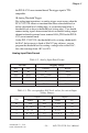
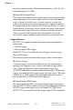
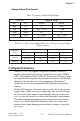
Table Of Contents
- Contents
- 1. Introduction
- 1.1 Features
- 1.2 Installation Guide
- 1.3 Accessories
- 2. Installation
- 2.1 Unpacking
- 2.2 Driver Installation
- 2.3 Hardware Installation
- 2.4 Device Setup & Configuration
- 2.5 Device Testing
- 3. Signal Connections
- 3.1 Overview
- 3.2 I/O Connector
- 3.3 Analog Input Connections
- 3.4 Analog Output Connections
- 3.5 Field Wiring Considerations
- 4. Software Overview
- 4.1 Programming Choices
- 4.2 DLL Driver Programming Roadmap
- 5. Principles of Operation
- 5.1 Analog Input Features
- 5.2 Analog Output Features
- 5.3 Digital I/O Features
- 5.4 Counter/Timer Features
- 6. Calibration
- 6.1 VR Assignment
- 6.2 A/D Calibration
- 6.3 D/A Calibration
- 6.4 Calibration Utility
- Appendix A. Specification
- Appendix B. Block Diagram
- Appendix C. Screw-terminal Board
- C. 1 Introduction
- C. 2 Features
- C. 3 Board Layout
- C.4 Pin Assignment
- C.5 Single-ended Connections
- C.6 Differential Connections
- Appendix D. Register Structure and Format
- D.1 Overview
- D.2 I/O Port Address Map
- D.3 A/D Single Value Acquisition - Write BASE+0
- D.4 Channel and A/D data - Read BASE + 0
- D.5 A/D Channel Range Setting - Write BASE+2
- D.6 MUX Control - Write BASE+4
- D.7 A/D Control/Status Register - Write/Read BASE+6
- D.8 Clear interrupt and FIFO - Write BASE+8
- D. 9 Interrupt and FIFO status - Read BASE+8
- D.10 D/A control/status register - Write/Read BASE+A
- D.11 D/A Channel 0/1 Data - Write BASE+C/E
- D.12 82C54 Counter Chip 0 - Write/Read BASE+10 to 16
- D.13 82C54 counter chip 1 - Write/Read BASE+18 to 1E
- D.14 Counter gate and clock control/status - Write/ Read BASE+20 to 26
- D.15 Digital I/O registers - Write/Read BASE+28
- D.16 Digital I/O configuration registers - Write/Read BASE+2A
- D.17 Calibration command registers - Write BASE+2C
- D.18 D/A Channel Data for Continuous Output Operation Mode - Write BASE+30
- Figures
- Figure 2-1: The Setup Screen of Advantech Automation Software
- Figure 2-2: Different options for Driver Setup
- Figure 2-3: The device name listed on the Device Manager
- Figure 2-4: The Advantech Device Installation utility program
- Figure 2-5: The I/O Device Installation dialog box
- Figure 2-6: The "Device(s) Found" dialog box
- Figure 2-7: The Device Setting dialog box
- Figure 2-8: The Device Name appearing on the list of devices box
- Figure 2-9: Analog Input tab on the Device Test dialog box
- Figure 2-10: Analog Input tab on the Device Test dialog box
- Figure 2-11: Analog Output tab on the Device Test dialog box
- Figure 2-12: Digital Input tab on the Device Test dialog box
- Figure 2-13: Digital Output tab on the Device Test dialog box
- Figure 2-14: Digital output tab on the Device Test dialog box
- Figure 3-1: I/O connector pin assignments for the PCI-1712/1712L
- Figure 3-2: Single-ended input channel connection
- Figure 3-3: Differential input channel connection - ground reference signal source
- Figure 3-4: Differential input channel connection - floating signal source
- Figure 3-5: Analog output connections
- Figure 5-1: Post-Trigger Acquisition Mode
- Figure 5-2: Delay-Trigger Acquisition Mode
- Figure 5-3: About-Trigger Acquisition Mode
- Figure 5-4: Pre-Trigger Acquisition Mode
- Figure 5-5: PCI-1712/1712L Sample Clock Source
- Figure 5-6: Frequency measurement
- Figure 6-1: PCI-1712/1712L VR1 & TP5
- Figure 6-2: Selecting the device you want to calibrate
- Figure 6-3: Warning message before start calibration
- Figure 6-4: Auto A/D Calibration Dialog Box
- Figure 6-5: A/D Calibration Procedure 1
- Figure 6-6: A/D Calibration Procedure 2
- Figure 6-7: A/D Calibration Procedure 3
- Figure 6-8: A/D Calibration is finished
- Figure 6-9: Range Selection in D/A Calibration
- Figure 6-10: Calibrating D/A Channel 0
- Figure 6-11: Calibrating D/A Channel 1
- Figure 6-12: D/A Calibration is finished
- Figure 6-13: Selecting Input Rage in Manual A/D Calibration panel
- Figure 6-14: Adjusting registers
- Figure 6-15: Selecting D/A Range and
- Figure 6-16: Selecting D/A Range and Choosing Output Voltage
- Figure 6-17: Adjusting registers
- Figure C-1: PCLD-8712 board layout
- Figure C-2: CN2 pin assignments for the PCLD-8712
- Tables
- Table 3-1: I/O Connector Signal Description (Part 1)
- Table 3-1: I/O Connector Signal Description (Part 2)
- Table 3-1: I/O Connector Signal Description (Part 3)
- Table 5-1: Gains and Analog Input Range
- Table 5-2: Analog Input Data Format
- Table 5-3: The corresponding Full Scale values for various Input Voltage Ranges
- Table 5-4: Analog Output Data Format
- Table 5-5: The corresponding Full Scale values for various Output Voltage Ranges
- Table D-1: PCI-1712/1712L register format (Part 1)
- Table D-1: PCI-1712/1712L register format (Part 2)
- Table D-1: PCI-1712/1712L register format (Part 3)
- Table D-2: Register for channel number and A/D data
- Table D-3: Register for A/D channel range setting
- Table D-4: Gain Codes for the PCI-1712/1712L
- Table D-5: Register for multiplexer control
- Table D-6: Register for A/D control/status
- Table D-7: Analog Input Acquisition Mode
- Table D-8: Register for clear interrupt and FIFO
- Table D-9: Register for interrupt and FIFO status
- Table D-10: Register for D/A control
- Table D-11: Analog output operation mode
- Table D-12: Register for D/A channel 0/1 data
- Table D-13: Register for 82C54 counter chip 0
- Table D-14: Register for 82C54 counter chip 1
- Table D-15: Register for counter gate and clock control/status
- Table D-16 : Table of Cn1 to Cn0 register
- Table D-17: Table of Gn1 to Gn0 register
- Table D-18: Table for CLK_SEL1 to CLK_SEL0 register
- Table D-19: Register for Digital I/O
- Table D-20: Register for digital I/O configuration
- Table D-21: Register for digital I/O configuration
- Table D-22: Register for calibration command
- Table D-23: Calibration command
- Table D-24: Register for D/A channel data
– 43 –
Chapter 5
PCI-1712/1712L User’s Manual
Advantech Co., Ltd.
www.advantech.com
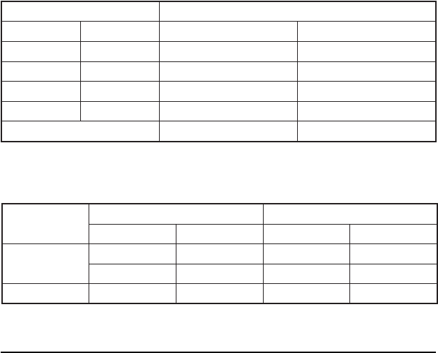
Analog Output Data Format
Table 5-4: Analog Output Data Format
Table 5-5: The corresponding Full Scale values for various Output
Voltage Ranges
5.3 Digital I/O Features
The PCI-1712/1712L supports 16 digital I/O channels. These I/O
channels are divided into two bytes: specifically a low byte, DIO0 to
DIO7; and a high byte, DIO8 to DIO15. You can use each byte as either
an input port or an output port by configuration register; and all eight
channels of the byte have the same configuration. For detailed
information, please refer to Appendix D.16 Digital I/O configuration
registers.
In digital I/O function, you do not need to specify the clock source or
trigger source. When you want to output data, you just need to write
the data to the digital output channel through software. In the same
way, you can use software to read the data from digital input channel.
The default configuration after power on, hardware reset or software
reset is to set all the digital I/O channels to logic-low so that users
need not worry about damaging external devices during system start
up or reset.
edocA/D egatloVgnippaM
.xeH .ceD ralopinU ralopiB
h000 d0 0 2/SF-
hFF7 d7402 BSL1-2/SF BSL1-
h008 d8402 2/SF 0
hFFF d5904 BSL1-SF BSL1-2/SF
BSL1 6904/SF 6904/SF
ecnerefeR
ecruoS
ralpinU ralopiB
egnaR SF egnaR SF
lanretnI
V5~0 5 V5± 01
V01~0 01 V01± 02
lanretxE Vx~0 x Vx± x2