
User's Manual


BT860
Datasheet
Embedded Wireless Solutions Support Center:
http://ews-support.lairdtech.com
www.lairdtech.com/bluetooth
5
© Copyright 2017 Laird. All Rights Reserved
Americas: +1-800-492-2320
Europe: +44-1628-858-940
Hong Kong: +852 2923 0610
3 B
LOCK
D
IAGRAM AND
D
ESCRIPTIONS
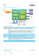
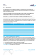
Figure 1: BT860 Module block diagram
CYW20704A2
(Main chip)
The BT860 is based on CYW20704A2 dual mode chip. The chip is a single-chip radio with on-
chip LDO regulators and baseband IC for Bluetooth 2.4 GHz systems including EDR to
3 Mbps.
Dedicated signal and baseband processing is included for full Bluetooth operation. The chip
provides I
2
S/PCM and USB interfaces. There are two general purpose I/Os be configured for
proprietary of Cypress GCI used and a general purpose I/O can be configured for
scan/inquire/paging/data traffic of indicator. There three I/Os pins are controlled by
firmware.
Antenna BT860 – The antenna is a ceramic monopole chip antenna.
Band Pass
Filter
The band pass filter filters the out-of-band emissions from the transmitter to meet the
specific regulations for type approvals of various countries.
EEPROM There are 512 k bits EEPROM embedded on the BT860 module which can be used to store
parameters, such as BD_ADDR, USB enumeration information, maximum TX power, PCM
configuration, USB product ID, USB vendor ID, and USB product description. With that, the
BT860 module can support UHE/HCI Proxy mode.
Crystal The embedded 40 MHz crystal is used for generating the clock for the entire module.