
User's Manual
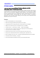


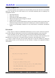


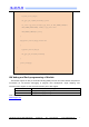


Table Of Contents

Block diagram:
Pin Description of Module
(
Top View
)
:
Pin No.
Name
Description
Note
1
P0.08
I/O
2
P0.09
I/O
3
P0.12
I/O
4
SWDIO
Debug and flash programming I/O
5
SWCLK
Debug and flash programming I/O
6
P0.17
I/O
7
P0.18
I/O
8
P0.19
I/O
9
GND
Power Ground
10
VDD
Power Supply
11
P0.25
I/O
12
P0.26
I/O
ADC IN 0
13
P0.27
I/O
ADC IN 1
14
P0.28
I/O
15
P0.29
I/O
Note 1: An internal 4.7μF bulk capacitor has been included on the module. it is good design
practice to add additional bulk capacitance(e.g 10uF) as required for your application.
COPYRIGHT ©2016 ALL RIGHTS RESERVED XunTong Tech TEL: +86 755 26675941 E-mail: nrf@freqchina.com
3