
User's Manual
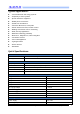


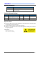
Table Of Contents

Block diagram:
General Purpose I/O:
The general purpose I/O is organized as one port enabling access and control of the 32 available
GPIO pins through one port. Each GPIO can be accessed individually with the following user
configurable features:
Input/output direction
Output drive strength
Internal pull-up and pull-down resistors
Wake-up from high or low level triggers on all pins
Trigger interrupt on all pins
All pins can be used by the PPI task/event system; the maximum number of pins that can be
interfaced through the PPI at the same time is limited by the number of GPIOTE channels
All pins can be individually configured to carry serial interface or quadrature demodulator
signals
HW debug and flash programming of Module:
The Module support the two pin Serial Wire Debug (SWD) interface and offers flexible and powerful
mechanism for non-intrusive debugging of program code. Breakpoints, single stepping, and
instruction trace capture of code execution flow are part of this support.
Pin Flash Program interface
SWDIO Debug and flash programming I/O
SWCLK
Debug and flash programming I/O
This is the hardware debug and flash programming of module, J-Link Lite support, please refer
www.segger.com
.
COPYRIGHT ©2016 ALL RIGHTS RESERVED XunTong Tech TEL: +86 755 26675941 E-mail: nrf@freqchina.com
4