
User's Manual

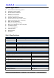

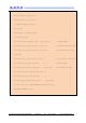
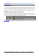

Table Of Contents

14
P0.29
I/O
ADC IN
15
P0.30
I/O
ADC IN
Note 1: P0.20 and P0.24 are reserved for PA control internal.
Note 2: An internal 4.7μF bulk capacitor has been included on the module. it is good design
practice to add additional bulk capacitance(e.g 10uF) as required for your application.
General Purpose I/O:
The general purpose I/O is organized as one port enabling access and control of the 32 available
GPIO pins through one port. Each GPIO can be accessed individually with the following user
configurable features:
Input/output direction
Output drive strength
Internal pull-up and pull-down resistors
Wake-up from high or low level triggers on all pins
Trigger interrupt on all pins
All pins can be used by the PPI task/event system; the maximum number of pins that can be
interfaced through the PPI at the same time is limited by the number of GPIOTE channels
All pins can be individually configured to carry serial interface or quadrature demodulator
signals
PA control:
Additional logic signals are needed to control TX PA and RX LNA. On the nRF51 there was an
option to use the VDD_PA pin to detect when the radio was in TX mode, but this is not an option on
the nRF52, making the SoftDevice solution necessary. The S132 SoftDevice for the nRF52 has
support for enable/disable switching of external Power Amplifiers (PA) and LNA using GPIO pins.
On the module, P0.20 and P0.24 are reserved to control PA and LNA, so these two pins can Not
be allocated to other usage.
The truth table of PA/LNA control signals as bellow:
PIN24 PIN20 PA status
1 0 TXEN
0 1 RXEN
0 0 IDLE
1 1 INVALID
The following function can be used to enable PA/LNA signal with P0.20 and P0.24. Add this
function to your project and call it after ble_stack_init():
static void pa_assist(uint32_t gpio_pa_pin,uint32_t gpio_lna_pin)
{
ret_code_t err_code;
COPYRIGHT ©2016 ALL RIGHTS RESERVED XunTong Tech TEL: +86 755 26675941 E-mail: nrf@freqchina.com
4