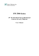
FW-7890 Series 19” 2U Intel Dual Xeron Rackmount Network Security Platform User’s Manual
Copyright and Disclaimers © Copyright 2004 - Lanner Electronics Inc. All Rights Reserved The contents in this publication have been thoroughly checked and considered accurate. The publisher and manufacturer of this product, Lanner Electronics, is not responsible for any violation of patents or other rights of third parties resulting from its use.
Federal Communications Commission (FCC) Statement This Equipment has been tested and found to comply with the limits for a Class A digital device, pursuant to Part 15 of the FCC rules. These limits are designed to provide reasonable protection against harmful interference when the equipment is operated in a commercial environment.
Safety Instructions The following information relates to the safety of installation and maintenance personnel. Read all instructions before attempting to unpack, install or operate this equipment, especially before connecting the power adapter. Please keep the following in mind as you unpack and install this equipment: Always follow basic safety precautions to reduce the risk of fire, electrical shock and injury to persons.
Getting Technical Assistance Should you encounter questions or problems with your FW-7890, Lanner Electronics is ready to assist you within the guidelines of our product support programs. First, check the electronic product documentation for assistance.
Table of Contents Copyright and Disclaimers....................................................................................................ii Trademark Acknowledgments...............................................................................................ii Radio Frequency Emissions Notice..................................................................... ii Safety Instructions ...............................................................................................
LCD Module and Key Pad For FW-7890...........................................................................44 A p p e n d i x E...................................................................................................................44 LAN Bypass Function .........................................................................................................
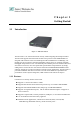
Chapter 1 Getting Started 1.1 Introduction Figure 1 – FW-7890 Outlook The FW-7890 is a 2U rackmount network security solution targeting the Enterprise market. The FW-7890 supports dual socket 604 for Intel Xeon processor with 800MHz FSB. It is designed with an Intel E7520 as its northbridge and Intel 6300ESB as its southbridge.; All Gigabit ports to be connected from the northbridge with six PCI-E x4, ensuring maximum throughput and performance.
1.2 Technical Specifications Model Name FW-7890A FW-7890B SBC SBC CPU Chipset Security Processor MB-X77A MB-X77B Dual Intel ® Xeon Processor, up to 3.
1.3 Packing Contents Carefully unpack your package and make sure that you have the following items. FW-7890 Network security Platform x 1 pcs Console cable(RJ-45) x 1 pcs 1.8 meters long cross-over Ethernet cable x 1 pcs 1.
1.4 MB-X77 System Board MB-X77 is the system board bundled with the FW-7890 Network security platform. The succeeding sections list all MB-X77 related jumper settings and connector pin assignments. 1.4.
1.4.2 Jumper Settings and I/O Connector The onboard jumper settings and I/O connector of MB-X77 are custom-tailored to fit the FW-7890 functionality. Changing the jumper settings may result in system malfunction or unforeseen damages. Jumper Settings and I/O Connector Summary for MB-X77 JUMPER FUNCTION PLRS1 Power LED,HD LED,Reset,Speaker Connector(11 Pin 2.54mm) PKMB1 PS/2 Keyboard & Mouse Connector (2x4 Header 2.54 mm) CMOS1 Clear CMOS Data IDEB1 IDE Interface Connector (40 Pin 2.
PLRS1:Power LED,HD LED,Reset,Speaker Connector(11 Pin 2.54mm) PIN NO. DESCRIPTION 1 Power LED + 2 Power LED + 3 GND 4 HDD LED + 5 HDD LED - 6 RESET SW + 7 RESET SW – (GND) 8 External Speaker - 9 Internal Buzzer - 10 NC 11 External Speaker + Default : 8-9 (ON) Internal Buzzer PKMB1:PS/2 Keyboard & Mouse Connector (2x4 Header 2.54mm ) PIN NO. DESCRIPTION PIN NO.
5 Data 6 6 Data 9 7 Data 5 8 Data 10 9 Data 4 10 Data 11 11 Data 3 12 Data 12 13 Data 2 14 Data 13 15 Data 1 16 Data 14 17 Data 0 18 Data 15 19 Ground 20 KEY 21 DMA REQ# 22 Ground 23 IOW # 24 Ground 25 IOR # 26 Ground 27 IOCHRDY 28 Ground 29 DMA ACK # 30 Ground 31 Interrupt 32 NC 33 SA1 34 PD80P / SD80P 35 SA0 36 SA2 37 HDC CS0 # 38 HDC CS1 # 39 HDD Active LED # 40 Ground 40 2 39 1 IDEB1 FAN1~3 : 3 Pin FAN Connector Pin No.
FAN4~6 : 3 Pin FAN Connector Pin No.
COMB1: Serial Port #2 Connector ( Header ) PIN NO DESCRIPTION 2 10 RS-232 1 Data Carrier Detect (DCDB #) 2 Data Set Ready (DSRB #) 3 Receive Data (RXDB) 4 Request To Send (RTSB #) 5 Transmit Data (TXDB) 6 Clear To Send (CTSB #) 7 Data Terminal Ready (DTRB #) 8 Ring Indicator (RIB #) 9 Ground 10 KEY 9 1 COMB1 LPTA1:Parallel Connector (26 Pin 2.00mm Pitch Header ) PIN NO. DESCRIPTION PIN NO.
PIN NO. DESCRIPTION PIN NO. DESCRIPTION 1 +3.3V 13 +3.3V 2 +3.3V 14 -12V 3 Ground 15 Ground 4 +5V 16 PSON- 5 Ground 17 Ground 6 +5V 18 Ground 7 Ground 19 Ground 8 Power Good 20 NC 9 Stand-By 5V 21 +5V 10 +12V 22 +5V 11 +12V 23 +5V 12 +3.3V 24 Ground PSC1 PCIB1:124 Pin Mini PCI Socket Pin No. Description Pin No.
25 CLK 26 RST 27 GROUND 28 +3.3V 29 REO 30 GNT 31 +3.3V 32 GROUND 33 AD31 34 PME 35 AD29 36 RESERVED 37 GROUND 38 AD30 39 AD27 40 +3.3V 41 AD25 42 AD28 43 RESERVED 44 AD26 45 C_BE-3 46 AD24 47 AD23 48 IDSEL 49 GROUND 50 GROUND 51 AD21 52 AD22 53 AD19 54 AD20 55 GROUND 56 PAR 57 AD17 58 AD18 59 C_BE-2 60 AD16 61 IRDY 62 GROUND 63 +3.3V 64 FRAME 65 CLKRUN 66 TRDY 67 SERR 68 STOP 69 GROUND 70 +3.
91 AD5 92 AD4 93 RESERVED 94 AD2 95 AD3 96 AD0 97 +5V 98 RESERVED-WIP 99 AD1 100 RESERVED-WIP 101 GROUND 102 GROUND 103 AC_SYNC 104 M66EN 105 AC_SDATA_IN 106 AC_SDATA_OUT 107 AC_BIT_CLK 108 AC_CODEC_ID0 109 AC_CODEC_ID1 110 AC_RESET 111 MOD_AUDIO_M 112 RESERVED 113 AUDIO_GND 114 GROUND 115 SYS_AUDIO_OU 116 SYS_AUDIO_IN 117 SYS_AUDIO_OU 118 SYS_AUDIO_IN 119 AUDIO_GND 120 AUDIO_GND 121 RESERVED 122 MPCIACT 123 VCC5VA 124 3.
PCIXA1: 184 Pin 3V PCIX Socket comments Pin Side B Side A 1 -12V TRST# 2 TCK +12V 3 Ground TMS 4 TDO TDI 5 +5V +5V 6 +5V INTA# 7 INTB# INTC# 8 INTD# +5V 9 PRSNT1# Reserved 10 Reserved +3.3V(I/O) 11 PRSNT2# Reserved 32-bit connector start 12 CONNECTOR KEY 3.3 volt key 13 CONNECTOR KEY 3.3 volt key 14 Reserved 3.3Vaux 15 Ground RST# 16 CLK +3.3V(I/O) 17 Ground GNT# 18 REQ# Ground 19 +3.3V(I/O) PME# 20 AD﹝31﹞ AD﹝30﹞ 21 AD﹝29﹞ +3.
30 AD﹝19﹞ Ground 31 +3.3V AD﹝18﹞ 32 AD﹝17﹞ AD﹝16﹞ 33 C/BE﹝2﹞# +3.3V 34 Ground FRAME# 35 IRDY# Ground 36 +3.3V TRDY# 37 DEVSEL# Ground 38 Ground STOP# 39 LOCK# +3.3V 40 PERR# Reserved* 41 +3.3V Reserved* 42 SERR# Ground 43 +3.3V PAR 44 C/BE﹝1﹞# AD﹝15﹞ 45 AD﹝14﹞ +3.3V 46 Ground AD﹝13﹞ 47 AD﹝12﹞ AD﹝11﹞ 48 AD﹝10﹞ Ground 49 M66EN AD﹝09﹞ 66MHZ/gnd 50 Ground Ground 5 volt key 51 Ground Ground 5 volt key 52 AD﹝08﹞ C/BE﹝0﹞# 53 AD﹝07﹞ +3.
CONNECTOR KEY 63 Reserved Ground 64 Ground C/BE﹝7﹞# 65 C/BE﹝6﹞# C/BE﹝5﹞# 66 C/BE﹝4﹞# +3.3V(I/O) 67 Ground PAR64 68 AD﹝63﹞ AD﹝62﹞ 69 AD﹝61﹞ Ground 70 +3.3V(I/O) AD﹝60﹞ 71 AD﹝59﹞ AD﹝58﹞ 72 AD﹝57﹞ Ground 73 Ground AD﹝56﹞ 74 AD﹝55﹞ AD﹝54﹞ 75 AD﹝53﹞ +3.3V(I/O) 76 Ground AD﹝52﹞ 77 AD﹝51﹞ AD﹝50﹞ 78 AD﹝49﹞ Ground 79 +3.3V(I/O) AD﹝48﹞ 80 AD﹝47﹞ AD﹝46﹞ 81 AD﹝45﹞ Ground 82 Ground AD﹝44﹞ 83 AD﹝43﹞ AD﹝42﹞ 84 AD﹝41﹞ +3.
PS4S1~2:4-Pin Power Connector (Small-4P ) Pin No. Description 1 5V 2 Ground 3 Ground 4 12V PS4S1 12 34 PS8P1:8-Pin Power Connector (Xeon-8P Male ) Pin No. Description Pin No. Description 1 Ground 5 +12V 2 Ground 6 +12V 3 Ground 7 +12V 4 Ground 8 +12V SATAB1 : 180º SATA CONNECTOR Pin No. Description 1 GND 2 TX_P 3 TX_M 4 GND 5 RX_M 6 RX_P 7 GND VR1:Control Sound PIN NO.
PME1:One PME1 Connector supports Wake-on-Lan PIN DESCRIPTION 1 3VSTB 2 PME- 3 GND LUSBCOM1:BOX_HEADER_2X20_2.00_DIP Pin No. Description Pin No.
1 12V 2 VCC3 3 12V 4 VCC3 5 12V 6 VCC3 7 RELAY_C 8 VCC3 9 VCC3AUX 10 VCC3 11 VCC 12 VCC 13 WAKE 14 TCK 15 PRSNT1 16 SMCLK 17 TRST 18 SMDAT 19 TDO 20 TDI 21 BTX3- 22 TMS 23 BTX3+ 24 BRX3- 25 GND 26 BRX3+ 27 BTX2- 28 GND 29 BTX2+ 30 BRX2- 31 GND 32 BRX2+ 33 BTX1- 34 GND 35 BTX1+ 36 BRX1- 37 GND 38 BRX1+ 39 BTX0- 40 GND 41 BTX0+ 42 BRX0- 43 GND 44 BRX0+ Key Key Key Key 45 GND 46 BCLK- 47 GND 48 BCLK+ 49 ATX3-
55 ATX2- 56 ARX3+ 57 ATX2+ 58 GND 59 GND 60 ARX2- 61 ATX1- 62 ARX2+ 63 ATX1+ 64 GND 65 GND 66 ARX1- 67 ATX0- 68 ARX1+ 69 ATX0+ 70 GND 71 GND 72 ARX0- 73 GND 74 ARX0+ 75 ACLK- 76 GND 77 ACLK+ 78 GND 79 GND 80 PWRGD USBF1:USB Port #1 & #2 Connector 2x5 Pin 2.
1.5 FW-7890 19” 2U Rackmount Firewall Mechanisms This section of the manual describes the mechanical and device nomenclature of FW-7890. 1.5.1 Face Panel LCM USB Console LED Status Hard disk Tray Keypad LAN Connector Figure 5 – FW-7890 Face Panel Face Panel LED Status and Behavior The following table lists and explains the behavior of each LED on the FW-7890 front panel.
Redundant Power Supply 1.5.3 Rear View System Fan Power Switch Power Mute Switch PCI-X Slot Figure 6 – FW-7890 Rear View Power Switch: Click the Power Switch , and the system will be power on. Power Mute Switch: When there is a power supply failure, the system will be alarm. Only click the power mute switch and the system will stop to alarm. Faulty or improper use of the power adaptor may cause permanent damage to the power supply and the FW-7890.
Chapter 2 FW-7890 Hardware Installation Guide 2.1 Hardware Installation Guide - CPU Installation If you plug in single CPU in FW-7890, be notes to put in CPU1. CPU1 CPU2 - System Memory Step 1: The DIMM slot has a notch, the DIMM memory module only fit in one direction. Step 2: Align the memory notch to the module and push the memory into the DIMM socket Step 1 Step 2 Be notes that it is the dual channel DDR II memory interface, so it needs to plug-in from one of the Blue DIMM first.
- Installing Compact Flash Card Step 1: Insert the compact flash card into the slot carefully as shown in the picture. Step 1 - Installing the Mini-PCI Card Step 1: Insert the PCI expansion card into the mini-PCI slot at 45 degree. Step 2: Push down the PCI expansion card and the PCI expansion card is clicked together completely with the PCI expansion slot.
Chapter 3 Award BIOS Setup 3.1 BIOS Setup Award‘s ROM BIOS provides a built-in Setup program that allows users to modify the basic system configuration and settings. The modified data will be stored in a battery-backed CMOS RAM so that this data will be retained even when the power is turned off. In general, the information saved in the CMOS RAM remains unchanged unless there is a configuration change in the system, such as hard drive replacement or new equipment installment.
Main Menu - Quit and not save changes into CMOS Status Page Setup Menu and Option Page Setup Menu - Exit current page and return to Main Menu <+/PgUp> Increase the numeric value or make changes <-/PgDn> Decrease the numeric value or make changes General help, only for Status Page Setup Menu and Option Page Setup Menu Item Help Restore the previous CMOS value from CMOS, only for Option Page Setup Menu Load the Optimized Defaults System Information Save al
Note that a brief description of each highlighted selection appears at the bottom of the screen. Standard CMOS Features Use this menu for basic system configuration. Advanced BIOS Features Use this menu to set the Advanced Features available on your system. Advanced Chipset Features Use this menu to change the values in the chipset registers and optimize your system's performance. Integrated Peripherals Use this menu to specify your settings for integrated peripherals.
3.3 Standard CMOS Features The items in Standard CMOS Setup Menu are divided into 9 categories. Each category includes no, one or more than one setup items. Use the arrow keys to highlight the item and then use the or keys to select the value you want in each item. Item Options Date Month DD YYYY Time IDE Channel 0 HH : MM : SS Options are in its sub menu Description Set the system date.
Master IDE Channel 0 Slave Options are in its sub menu IDE Channel 1 Master IDE Channel 2 Master Options are in its sub menu Options are in its sub menu Halt On All Errors No Errors All, but Keyboard All, but Diskette All, but Disk/Key Base Memory N/A Extended Memory N/A Total Memory N/A detailed options Press to enter the sub menu of detailed options Press to enter the sub menu of detailed options Press to enter the sub menu of detailed options Select the situation in wh
Access Mode Cylinder Head Precomp Landing zone Sector CHS LBA Large Auto Min = 0 Max = 65535 Min = 0 Max = 255 Min = 0 Max = 65535 Min = 0 Max = 65535 Min = 0 Max = 255 Choose the access mode for this hard disk Set the number of cylinders for this hard disk. Set the number of read/write heads **** Warning: Setting a value of 65535 means no hard disk **** Number of sectors per track 3.4 Advanced BIOS Features This section allows you to configure your system for basic operation.
Disabled processors mode supported. Disables CPU Hyper Threading Feature. Quick Power On Self Test : The default setting is “Enabled”. This speeds up the Power On Self Test (POST) by skipping some items that are normally checked during the full POST. If your system is functioning normally, you can choose this feature to speed up the booting process. First / Second / Third / Other Boot Device : The BIOS attempts to load the operating system from the devices in the sequence selected in these items.
Agent after Boot : Keep Agent after OS Boot.Configuration options: Enabled / Disabled Shadow Areas : These categories determine whether option ROMs will be copied to RAM, Enabled Disabled Optional shadow is enabled Optional shadow is disabled Full Screen LOGO Show: Show full screen logo during BIOS bootup process. Configuration options: Enabled/Disabled 3.
Memory Hole At 15M-16M: You can reserve this area of system memory for ISA adapter ROM. When this area is reserved, it cannot be cached. The user information of peripherals that need to use this area of system memory usually discusses their memory requirements. Delay Prior to Thermal : The Delay Prior To Thermal BIOS feature controls the activation of the Thermal Monitor's automatic mode. It allows you to determine when the Thermal Monitor should be activated in automatic mode after the system boots.
On-Chip (Primary/Secondary) PCI IDE : The Intel 82C440BX chipset contains a PCI IDE interface with support for two IDE channels. Select Enabled to activate the primary and/or secondary IDE interface. Select Disabled to deactivate this interface, if you install a primary and/or secondary add-in IDE interface. On-Chip Serial ATA This item allows you to configure your serial ATA devices if present. Disabled Auto Combined Mode Enhanced Mode SATA First Disable SATA controller. Auto arrange by BIOS.
USB Mouse Support: Select Enabled if you need to use a USB inferfaced Mouse in the operating system SuperIO Device : Scroll to this item and press to view the following screen: Watch Dog : Enable / Disable the Watch dog function. By Pass Function : Enable / Disable the LAN By Pass Function LPT/LCM CONTROL :Use this option to enable and configure or disable the LPT/LCM port present on the evaluation board.
3.7 Power Management Setup The Power Management Setup allows you to configure you system to most effectively save energy while operating in a manner consistent with your own style of computer use. ACPI Function : This item allows you to enable or disable the Advanced Configuration and Power Management (ACPI). The settings are “Enabled” and “Disabled”. Power Management : This category allows you to select the type (or degree) of power saving and is directly related to the following modes: 1.
V/H SYNC+Blank Blank Screen DPMS This selection will cause the system to turn off the vertical and horizontal synchronization ports and write blanks to the video buffer. This option only writes blanks to the video buffer. Initial display power management signaling. Suspend Type Select the Suspend Type.Configuration options: PWRON Suspend / Stop Grant Suspend Mode When enabled and after the set time of system inactivity, all devices except the CPU will be shut off.
3.8 PnP/PCI Configuration This section describes configuring the PCI bus system. PCI, or Personal Computer Interconnect, is a system which allows I/O devices to operate at speeds nearing the speed the CPU itself uses when communicating with its own special components. This section covers some very technical items and it is strongly recommended that only experienced users should make any changes to the default settings. Reset Configuration Data Normally, you leave this field Disabled.
3.9 PC Health Status CPU Temperature Detect CPU temperature automatically. System Temperature Detect System temperature automatically. FAN 1 / FAN 2 / FAN 3 Detect Fan1 / FAN2 speed status automatically . Vcore / +1.5V / +3.3V / +5V / +12V / -12V / -5V / +2.6V / VBAT Detect system' s voltage status automatically .
3.10 Load Optimized Defaults When you press on this item you get a confirmation dialog box with a message similar to: Load Optimized Defaults (Y/N) ? N 3.11 Supervisor/User Password Setting You can set either supervisor or user password, or both of then. The differences between are: Supervisor password: can enter and change the options of the setup menus. User password: just can only enter but do not have the right to change the options of the setup menus.
3.12 Save and Exit Setup Pressing on this item asks for confirmation: Save to CMOS and EXIT (Y/N)? Y Pressing “Y” stores the selections made in the menus in CMOS – a special section of memory that stays on after you turn your system off. The next time you boot your computer, the BIOS configures your system according to the Setup selections stored in CMOS. After saving the values the system is restarted again. 3.
Appendix A Power Supply Power Supply Specification AC Input Spec : VOLTAGE 90 ~ 264 VAC FULL RANGE Output Specifications Output Voltage Output Current Min. Output Current Max. Output Current Peak Regulation Load Regulation Line Output Ripple & Noise Max.[P-P] 5V 2 30.00 ± 5% ± 1% 50mV 12V 2 32.00 ± 5% ± 1% 120mV -5V 0.05 0.70 +5 ~ -10% ± 1% 120mV -12V 0.05 0.70 +5 ~ -10% ± 1% 120Mv 3.3V 1 24 ± 5% ± 1% 50mV +5VSB 0.
Appendix B Watchdog Timer Introduction Most systems need to be self-reliant. It's not usually possible to wait for someone to reboot them if there are some component wrong. Some system designs, such as space probes, are simply not accessible to human operators. If the system ever hangs, such systems are permanently disabled. In other cases, the speed with which a human operator might reset the system would be too slow to meet the uptime requirements of the product.
Appendix C Console Redirection Console redirection allows you to maintain a system from a remote location by re-directing keyboard input and text output through the serial port. This section will tell you how to use console redirection. 1. Please insert console cable between on FW-7890 and Remote Client System. 2. Setup BIOS in FW-7890.
Appendix D LCD Module and Key Pad For FW-7890 Purpose The purpose of this document is to provide installation information for the LCD module and key pad installed in the FW-7890. Specification overview The LCD module is designed to provide real-time operating status and configuration information for the system. You can reference the document in the Manual/Driver CD for detail specification. The path is under //LCM/LCD_Datasheet.pdf. The Driver and library is in the Manula/Driver CD.
2.Read_KeyPad(); =>This Function get the KeyPad number if user pressed key. =>Direct write function to your program. Ex. int a; a=Read_KeyPad(); Return Value: "1"=>The Upper Key "2"=>The Down Key "3"=>The Enter Key "4"=>The ESC Key 3.Show_Data(int Dp_Type1,int Dp_Type2,int Dp_Type3,int Dp_Type4, char *Showdata1, char *Showdata2); =>Show string Function.
Appendix E LAN Bypass Function Introduction The bypass function is used to link (or short) two indepent ehernet ports when the system crash or power off. That means if there are some condition in your system, with LAN Bypass function, it will not interrupt you network traffic. There are two communications states for the bypass function, one is Normal state and another is Bypass state. Lanner provide three states to enable LAN Bypass function. 1.
Terms and Conditions Date:2004.07.08 Warranty Policy 1. All products are warranted against defects in materials and workmanship for a period of two years from the date of your purchase. 2. The buyer will bear the return freight charges for goods returned for repair within the warranty period; whereas manufacturer will bear the after service freight charges back to user site. 3.
RMA Service Request Form When requesting RMA service, please fill out this RMA Service Request Form. Without this form your RMA will be REJECTED!!! RMA No: Reasons to Return: □ Repair(Please include failure details) □ Testing Purpose Company: Contact Person: Phone No. Purchased Date: Fax No.: Applied Date: Return Shipping Address: Shipping by: □ Air Freight □ Sea Item Item □ Express Model Name □ Others: Serial Number Problem Code *Problem Code: 01:D.O.A. 02: Second Time R.M.A.
PEXNSD01-040709 Version 1.