IAC-F848 Manual
IAC-F848 IAC-F848 Manual © Copyright 2007, Lanner Electronics, Inc. All rights reserved. This document contains proprietary information that is protected by copyright. No part of this document may be reproduced, transmitted, transcribed, stored in a retrieval system, or translated into any language in any form by any means without the written express of Lanner Electronics, Inc. The author and Lanner Electronics, Inc. have used their best efforts in preparing this manual.
IAC-F848 Safety Guidelines Follow these guidelines to ensure general safety: Keep the chassis area clear and dust-free during and after installation. Do not wear loose clothing or jewelry that could get caught in the chassis. Fasten your tie or scarf and roll up your sleeves. Wear safety glasses if you are working under any conditions that might be hazardous to your eyes. Do not perform any action that creates a potential hazard to people or makes the equipment unsafe.
IAC-F848 EMC Notice This equipment has been tested and found to comply with the limits for a Class A digital device, pursuant to Part 15 of the FCC Rules. These limits are designed to provide reasonable protection against harmful interference when the equipment is operated in a commercial environment. This equipment generates, uses, and can radiate radio frequency energy and, if not installed and used in accordance with the instruction manual, may cause harmful interference to radio communications.
IAC-F848 Contents Safety Guidelines....................................................................... 3 EMC Notice................................................................................. 4 Contents..................................................................................... 5 1. Product Overview.................................................................. 7 1.1 Product Introduction................................................................7 1.2Features and Benefits..........
IAC-F848 RMA Service . .............................................................................37 Requesting a RMA#.....................................................................37 RMA Service Request Form. ..........................................................
IAC-F848 1. Product Overview 1.1 Product Introduction IAC-F848 is a full-size PICMG 1.0 compliant SBC supporting an Intel Pentium 4 LGA775 processor. Built around the Intel 945G + ICH7 Chipset, the IAC-F848 offers a multitude of advanced connectivity features such as VGA / SATA / LAN / USB / CF / Mini-PCI and optional with Second LAN / Audio / LVDS / DVI / TV-Out / S-Video. 1.
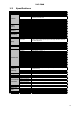
IAC-F848 1.3 Specifications FEATURE Platform Sy stem Memory Storage Interface Networking DESCRIPTION Form Factor Full-size, PICMG 1.
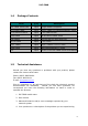
IAC-F848 1.4 Package Contents Item Q'ty Description IAC-F848 Series SBC 1pcs Single Board Computer LPT/COM Cable 1pcs 216C3 Cable (LPT&COM Bracket) 29cm ATX Feature Cable 1pcs 4-Pin Cable 40cm FDD Cable 1pcs 34-to-34Pin Cable 50cm IDE Cable 1pcs ATA100 40-Pin IDE with Key SATA Cable 2pcs 7-Pin 15cm PS/2 Cable 1pcs PS/2 Y Cable 5-Pin 13.5cm USB Cable 2pcs USB Cable/Bracket 2-Ports CD 1pcs CD V1.0 For IAC-F848 Driver and Manual 1.
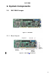
IAC-F848 2. System Components 2.1 IAC-F848 Images Figure 1 – IAC-F848 2.1.
IAC-F848 2.1.2 Dimensions (mm) Figure 3 – Dimensions 2.2 Settings and I/O Connectors The jumper settings and I/O connectors of the IAC-F848 board are specific to the IAC-F848. Changing these settings may result in malfunctions or damage to your system. CCMOS2: Clear CMOS Data DESCRIPTION CMOS Normal (Default) 1-2 Clear CMOS 2-3 COMA1: Pin header PIN NO. DESCRIPTION PIN NO.
IAC-F848 PK M1: PS/2 Keyboard & Mouse Connector PIN NO. DESCRIPTION PIN NO. DESCRIPTION 1 KBDT 2 MSDT 3 GND 4 +KBMS 5 KBCK 6 MSCK FDC A1: Floppy Interface Connector (34 Pin Header) PIN NO. DESCRIPTION PIN NO.
IAC-F848 ATX C1: For ATX Function PIN DESCRIPTION 1 GND 2 5VSB 3 GND 4 PS_ON# ATX PWR1: ATX 4 PIN CONNECTOR (FOR +12V VCORE) PIN DESCRIPTION PIN DESCRIPTION 1 GND 2 GND 3 +12V_CORE 4 +12V_CORE FPIO1: 4-Pin Power AND RESET FUNCTION PIN NO. DESCRIPTION 1 5VSB 2 GND 3 FP_SWIN 4 GND 5 RESET 2-3(POWER BUTTOM) 4-5(RESET) LPT A1:Parallel Connector (26 Pin 2.54mm Pitch Header) PIN NO. DESCRIPTION PIN NO.
IAC-F848 IRDA1: IRDA1 Connector PIN NO. DESCRIPTION 1 VCC 2 NC 3 IRRX 4 GND 5 IRTX CPU FAN1: 4 Pin FAN Connector PIN NO. DESCRIPTION 1 Ground 2 +12V 3 FAN Status 4 NC VGA1: External VGA Connector (12 Pin Header) PIN NO. DESCRIPTION PIN NO. DESCRIPTION 1 R 2 G 3 B 4 NC 5 GND 6 GND 7 GND 8 GND 9 NC 10 GND 11 NC 12 VGADDCDATA 13 H_SYNC 14 V_SYNC 15 VGADDCCLK IDE1: IDE Interface Connector PIN NO. DESCRIPTION PIN NO.
IAC-F848 37 HDC CS0 # 38 HDC CS1 # 39 HDD Active LED # 40 Ground CN1: Compact Flash Connector PIN DESCRIPTION PIN DESCRIPTION 1 GND 26 CD1- 2 DATA3 27 DATA11 3 DATA4 28 DATA12 4 DATA5 29 DATA13 5 DATA6 30 DATA14 6 DATA7 31 DATA15 7 CE1# 32 CE2# 8 A10 33 VS1# 9 OE# 34 IOR# 10 A9 35 IOW# 11 A8 36 WE# 12 A7 37 READY# 13 CFVCC3 38 CFVCC3 14 A6 39 CSEL 15 A5 40 VS2# 16 A4 41 RESET 17 A3 42 WAIT# 18 A2 43 INPACK# 19 A1 44 REG#
IAC-F848 31 +3.3V 32 GROUND 33 AD31 34 PME 35 AD29 36 RESERVED 37 GROUND 38 AD30 39 AD27 40 +3.3V 41 AD25 42 AD28 43 RESERVED 44 AD26 45 C_BE-3 46 AD24 47 AD23 48 IDSEL 49 GROUND 50 GROUND 51 AD21 52 AD22 53 AD19 54 AD20 55 GROUND 56 PAR 57 AD17 58 AD18 59 C_BE-2 60 AD16 61 IRDY 62 GROUND 63 +3.3V 64 FRAME 65 CLKRUN 66 TRDY 67 SERR 68 STOP 69 GROUND 70 +3.
IAC-F848 9 GND 17
IAC-F848 3. BIOS Setup BIOS Setup Award‘s ROM BIOS provides a built-in Setup program that allows users to modify the basic system configuration and settings. The modified data will be stored in a battery-backed CMOS RAM so that this data will be retained even when the power is turned off. In general, the information saved in the CMOS RAM remains unchanged unless there is a configuration change in the system, such as hard drive replacement or new equipment installment.
IAC-F848 3.1 Main Program Screen This screen provides access to the utility‘s various functions. Listed below is explanation of the keys displayed at the bottom of the screen: : Exit the utility. <↑↓→ ←>: Use arrow keys↑↓→ ← to move cursor to your desired selection. : General Help : Saves all changes made to Setup and exits program. Standard CMOS Setup: Use this menu for basic system configurations. Advanced BIOS Features: Use this menu to set the Advanced Features available on your system.
IAC-F848 Save & Exit Setup: Save CMOS value changes to CMOS and exit setup. Exit Without Saving: Abandon all CMOS value changes and exit setup. 3.2 Standard CMOS Setup When you select the “STANDARD CMOS SETUP” on the main program, the screen display will appears as: Standard CMOS Setup Screen The Standard CMOS Setup utility is used to configure the following components such as date, time, hard disk drive, floppy drive, display and memory.
IAC-F848 Cylinder: Number of cylinders Head: Number of heads Precomp: Write precom Landing Zone: Landing Zone Sector: Number of sectors Drive A and Drive B: Select the correct specifications for the diskette drive(s) installed in the computer. Note: 1. Not Installed could be used as an option for diskless workstations. 2. Highlight the listing after each drive name and select the appropriate entry.
IAC-F848 3.3 BIOS Features Setup When you select the “BIOS FEATURES SETUP” on the main program, the screen display will appear as: BIOS Features Setup Screen The following explains the options for each of the features as listed in the above menu: CPU Feature : When you press “Enter” on this item, you get CPU Feature screen as below: Delay Prior to Thermal: BIOS feature controls the activation of the Thermal Monitor's automatic mode.
IAC-F848 TM2 Bus Ratio: Represents the frequency (bus ratio)'of the throttled performance state that will be initiated when the on-die sensor gose from not hot to hot. TM2 Bus VID: Represents the voltage of the throttled performance state that will be initiated when the on-die sensor gose from not hot to hot. Limit CPUID Maxval: Enable Limit CPUID Maximum value to 3 when use older OS like NT4. Disable CPUID Limit for windows XP. C1E Function: Enable CPU Enhanced Halt (C1E) function.
IAC-F848 operating system from the devices in the sequence selected in these items. The settings are Floppy, LS/ZIP, HDD-0/HDD-1/HDD-2/HDD-3, SCSI, CDROM, LAN, and Disabled Boot Up Floppy Seek: The defaults setting is “Disabled”. When enabled, the BIOS will check whether there is a floppy disk drive installed. Boot Up NumLock Status: The default setting is “On”. If it set “Off”, the cursor controls will function on the numeric keypad. Typematic Rate Setting: The default setting is “Disabled”.
IAC-F848 3.4 CHIPSET FEATURES SETUP When you select the “CHIPSET FEATURES SETUP” on the main program, the screen display will appears as: Chipset Features Setup Screen Spread Spectrum: Enable/Disable to reduce the EMI of your motherboard by modulating the signals it generates so that the spikes are reduced to flatter curves.
IAC-F848 PEG Force X1: Enable/Disable the PCI Express X16 slot will be forced to run in the PCI Express X1 mode On-Chip Frame Buffer Size: Control the amount of system memory that is allocated to the integrated graphics processor when the system boots up. DVMT Mode: Intel's Dynamic Video Memory Technology (DVMT) takes that concept further by allowing the system to dynamically allocate memory resources according to the demands of the system at any point in time.
IAC-F848 3.5 INTEGRATED PERIPHERALS When you select the “INTEGRATED PERIPHERIALS” on the main program, the screen display will appears as: Integrated Peripherals Setup Screen On-Chip IDE Device: IDE HDD Block Mode: Speed up hard disk access by transferring multiple sectors of data per interrupt instead of using the usual single-sector transfer mode. IDE DMA Transfer Access: Enable/Disable DMA (Direct Memory Access) support for all IDE devices.
IAC-F848 interface. Select Disabled to deactivate this interface. On-Chip Secondary PCI IDE : The chipset contains a PCI IDE interface with support for two IDE channels. Select Enabled to activate the secondary IDE interface. Select Disabled to deactivate this interface. Primary / Secondary Master / Slave PIO : The four IDE PIO (Programmed Input/Output) fields let you set a PIO mode (0-4) for each of the four IDE devices that the onboard IDE interface supports.
IAC-F848 Super IO Device: Onboard FDD Controller : Select Enabled if your system has a floppy disk controller (FDC) installed on the system board and you want to use it. If you install add-in FDC or the system has no floppy drive, select Disabled in this field. The settings are “Enabled” and “Disabled”. Onboard Serial Port 1 / Port 2 : Select an address and corresponding interrupt for the first and second serial ports. The settings are “3F8/IRQ4”, “2E8/IRQ3”, “3E8/IRQ4”, “2F8/IRQ3”, “Disabled”, “Auto”.
IAC-F848 ACPI Function : This item allows you to enable or disable the Advanced Configuration and Power Management (ACPI). ACPI Suspend Type: You can select Suspend type to S1 or S3. S1is Power On Suspend. S3(STR) is Suspend To RAM. Run VGABIOS if S3 Resume: This item allows invoke VGA bios when resume from S3. Power Management: This option allows you to select the type (or degree) of power saving for Doze, Standby, and Suspend modes.
IAC-F848 DPMS: Allows the BIOS to control the video display card if it supports the DPMS feature. Video Off in suspend : Enable/Disable Video Off in suspend. Suspend Type: To select suspend type as “Stop Grant” or “PwrOn Suspend”. MODEM Use IRQ : Name the interrupt request (IRQ) line assigned to the modem (if any) on your system. Activity of the selected IRQ always awakens the system.
IAC-F848 FDD,COM,LPT Port: Enable/Disable this one of Reload Global Timer Events. PCI PIRQ[A-D]#: Enable/Disable this one of Reload Global Timer Events. 3.7 PNP/PCI CONFIGURATION Both the ISA and PCI buses on the CPU card use system IRQs & DMAs. You must set up the IRQ and DMA assignments correctly through the PnP/PCI Configuration Setup utility; otherwise the motherboard will not work properly.
IAC-F848 PCI/VGA Palette Snoop : This BIOS feature determines if your graphics card should allow VGA palette snooping by a fixed function display card. Maximum Payload Size: This determines the maximum TLP (Transaction Layer Packet) payload size that can be supported by the motherboard chipset's PCI Express controller. The TLP payload size determines the amount of data transmitted within each data packet 3.
IAC-F848 3.9 LOAD OPTIMIZED DEFAULTS When you press “Enter” on this item, you get a confirmation dialog box with a message similar to : Load Optimized Defaults (Y/N) ? N Pressing “Y” loads the default values that are factory settings for optimal performance system operations. 3.10 SET SUPERVISOR / USER PASSWORD The “SUPERVISOR/USER PASSWORD” utility sets the password. The SBC is shipped with the password disabled.
IAC-F848 35
IAC-F848 3.11 SAVE & EXIT SETUP Select this option and press the key to save the new setting information in the CMOS memory and continue with the booting process. 3.12 EXIT WITHOUT SAVING Select this option and press the key to exit the Setup Utility without recording any new values or changing old ones.
IAC-F848 Terms and Conditions Date:2007.03.19 Warranty Policy 1. All products are under warranty against defects in materials and workmanship for a period of one year from the date of purchase. 2. The buyer will bear the return freight charges for goods returned for repair within the warranty period; whereas the manufacturer will bear the after service freight charges for goods returned to the user. 3.
IAC-F848 RMA Service Request Form When requesting RMA service, please fill out the following form. Without this form enclosed, your RMA cannot be processed. Company: Reasons to Return: □ Repair(Please include failure details) □ Testing Purpose Contact Person: Phone No. Purchased Date: Fax No.: Applied Date: RMA No: Return Shipping Address: Shipping by: □ Air Freight □ Sea □ Others:________________ □ Express Item Model Name Item Problem Code Failure Status *Problem Code: 01:D.O.A.